SGLS244B May 2004 – December 2016 TLV2371-Q1 , TLV2372-Q1 , TLV2374-Q1
PRODUCTION DATA.
- 1 Features
- 2 Applications
- 3 Description
- 4 Revision History
- 5 Device Comparison Table
- 6 Pin Configuration and Functions
- 7 Specifications
- 8 Detailed Description
- 9 Application and Implementation
- 10Power Supply Recommendations
- 11Layout
- 12Device and Documentation Support
- 13Mechanical, Packaging, and Orderable Information
パッケージ・オプション
デバイスごとのパッケージ図は、PDF版データシートをご参照ください。
メカニカル・データ(パッケージ|ピン)
- D|8
- DBV|5
サーマルパッド・メカニカル・データ
- D|8
発注情報
7 Specifications
7.1 Absolute Maximum Ratings
over operating free-air temperature range (unless otherwise noted)(1)| MIN | MAX | UNIT | ||
|---|---|---|---|---|
| Supply voltage, VDD | 16.5 | V | ||
| Differential input voltage, VID | ±VDD | |||
| Input voltage, VI | –0.2 | VDD + 0.2 | V | |
| Input current, II | ±10 | mA | ||
| Output current, IO | ±100 | mA | ||
| Maximum junction temperature, TJ | 150 | °C | ||
| Storage temperature, Tstg | –65 | 150 | °C | |
(1) Stresses beyond those listed under Absolute Maximum Ratings may cause permanent damage to the device. These are stress ratings only, which do not imply functional operation of the device at these or any other conditions beyond those indicated under Recommended Operating Conditions. Exposure to absolute-maximum-rated conditions for extended periods may affect device reliability.
7.2 ESD Ratings
| VALUE | UNIT | ||||
|---|---|---|---|---|---|
| TLV2371-Q1 in DBV package | |||||
| V(ESD) | Electrostatic discharge | Human-body model (HBM), per AEC Q100-002(1) | All pins | ±2000 | V |
| Charged-device model (CDM), per AEC Q100-011 | All pins | ±500 | |||
| Corner pins (1, 3, 4, and 5) | ±750 | ||||
| TLV2371-Q1 in D package | |||||
| V(ESD) | Electrostatic discharge | Human-body model (HBM), per AEC Q100-002(1) | All pins | ±2000 | V |
| Charged-device model (CDM), per AEC Q100-011 | All pins | ±500 | |||
| Corner pins (1, 4, 5, and 8) | ±750 | ||||
| TLV2372-Q1 in D package | |||||
| V(ESD) | Electrostatic discharge | Human-body model (HBM), per AEC Q100-002(1) | All pins | ±2000 | V |
| Charged-device model (CDM), per AEC Q100-011 | All pins | ±500 | |||
| Corner pins (1, 4, 5, and 8) | ±750 | ||||
| TLV2374-Q1 in D and PW packages | |||||
| V(ESD) | Electrostatic discharge | Human-body model (HBM), per AEC Q100-002(1) | All pins | ±2000 | V |
| Charged-device model (CDM), per AEC Q100-011 | All pins | ±500 | |||
| Corner pins (1, 7, 8, and 14) | ±750 | ||||
(1) AEC Q100-002 indicates that HBM stressing shall be in accordance with the ANSI/ESDA/JEDEC JS-001 specification.
7.3 Recommended Operating Conditions
over operating free-air temperature range (unless otherwise noted)| MIN | MAX | UNIT | |||
|---|---|---|---|---|---|
| VDD | Supply voltage | Single supply | 2.7 | 16 | V |
| Split supply | ±1.35 | ±8 | |||
| VICR | Common-mode input voltage | 0 | VDD | V | |
| V(ON) | Turnon voltage level (relative to GND pin voltage) | 2 | V | ||
| V(OFF) | Turnoff voltage level (relative to GND pin voltage) | 0.8 | V | ||
| TA | Operating free-air temperature (Q-suffix) | –40 | 125 | °C | |
7.4 Thermal Information: TLV2371-Q1
| THERMAL METRIC(1) | TLV2371-Q1 | UNIT | ||
|---|---|---|---|---|
| DBV (SOT-23) | D (SOIC) | |||
| 5 PINS | 8 PINS | |||
| RθJA | Junction-to-ambient thermal resistance | 228.5 | 138.4 | °C/W |
| RθJC(top) | Junction-to-case (top) thermal resistance | 99.1 | 89.5 | °C/W |
| RθJB | Junction-to-board thermal resistance | 54.6 | 78.6 | °C/W |
| ψJT | Junction-to-top characterization parameter | 7.7 | 29.9 | °C/W |
| ψJB | Junction-to-board characterization parameter | 53.8 | 78.1 | °C/W |
| RθJC(bot) | Junction-to-case (bottom) thermal resistance | — | — | °C/W |
(1) For more information about traditional and new thermal metrics, see the Semiconductor and IC Package Thermal Metrics application report.
7.5 Thermal Information: TLV2372-Q1
| THERMAL METRIC(1) | TLV2372-Q1 | UNIT | |
|---|---|---|---|
| D (SOIC) | |||
| 8 PINS | |||
| RθJA | Junction-to-ambient thermal resistance | 138.4 | °C/W |
| RθJC(top) | Junction-to-case (top) thermal resistance | 89.5 | °C/W |
| RθJB | Junction-to-board thermal resistance | 78.6 | °C/W |
| ψJT | Junction-to-top characterization parameter | 29.9 | °C/W |
| ψJB | Junction-to-board characterization parameter | 78.1 | °C/W |
| RθJC(bot) | Junction-to-case (bottom) thermal resistance | — | °C/W |
(1) For more information about traditional and new thermal metrics, see the Semiconductor and IC Package Thermal Metrics application report.
7.6 Thermal Information: TLV2374-Q1
| THERMAL METRIC(1) | TLV2374-Q1 | UNIT | ||
|---|---|---|---|---|
| D (SOIC) | PW (TSSOP) | |||
| 14 PINS | 14 PINS | |||
| RθJA | Junction-to-ambient thermal resistance | 67 | 121 | °C/W |
| RθJC(top) | Junction-to-case (top) thermal resistance | 24.1 | 49.4 | °C/W |
| RθJB | Junction-to-board thermal resistance | 22.5 | 62.8 | °C/W |
| ψJT | Junction-to-top characterization parameter | 2.2 | 5.9 | °C/W |
| ψJB | Junction-to-board characterization parameter | 22.1 | 62.2 | °C/W |
| RθJC(bot) | Junction-to-case (bottom) thermal resistance | — | — | °C/W |
(1) For more information about traditional and new thermal metrics, see the Semiconductor and IC Package Thermal Metrics application report.
7.7 Electrical Characteristics
at specified free-air temperature, VDD = 2.7 V, 5 V, and 15 V (unless otherwise noted)| PARAMETER | TEST CONDITIONS | MIN | TYP | MAX | UNIT | |||
|---|---|---|---|---|---|---|---|---|
| DC PERFORMANCE | ||||||||
| VIO | Input offset voltage | VIC = VDD/2, VO = VDD/2, RS = 50 Ω | TA = 25°C | 2 | 4.5 | mV | ||
| TA = –40°C to 125°C | 6 | |||||||
| αVIO | Offset voltage drift | VIC = VDD/2, VO = VDD/2, RS = 50 Ω, TA = 25°C | 2 | µV/°C | ||||
| CMRR | Common-mode rejection ratio | VDD = 2.7 V | VIC = 0 to VDD, RS = 50 Ω |
TA = 25°C | 50 | 68 | dB | |
| TA = –40°C to 125°C | 49 | |||||||
| VIC = 0 to VDD – 1.35 V, RS = 50 Ω |
TA = 25°C | 53 | 70 | |||||
| TA = –40°C to 125°C | 54 | |||||||
| VDD = 5 V | VIC = 0 to VDD, RS = 50 Ω |
TA = 25°C | 55 | 72 | ||||
| TA = –40°C to 125°C | 54 | |||||||
| VIC = 0 to VDD – 1.35 V, RS = 50 Ω |
TA = 25°C | 58 | 80 | |||||
| TA = –40°C to 125°C | 57 | |||||||
| VDD = 15 V | VIC = 0 to VDD, RS = 50 Ω |
TA = 25°C | 64 | 82 | ||||
| TA = –40°C to 125°C | 63 | |||||||
| VIC = 0 to VDD – 1.35 V, RS = 50 Ω |
TA = 25°C | 67 | 84 | |||||
| TA = –40°C to 125°C | 66 | |||||||
| AVD | Large-signal differential voltage amplification | VO(PP) = VDD/2, RS = 10 Ω |
VDD = 2.7 V | TA = 25°C | 95 | 106 | dB | |
| TA = –40°C to 125°C | 76 | |||||||
| VDD = 5 V | TA = 25°C | 80 | 110 | |||||
| TA = –40°C to 125°C | 82 | |||||||
| VDD = 15 V | TA = 25°C | 77 | 83 | |||||
| TA = –40°C to 125°C | 79 | |||||||
| INPUT | ||||||||
| IIO | Input offset current | VDD = 15 V, VIC = VDD/2, VO = VDD/2 | TA = 25°C | 1 | 60 | pA | ||
| TA = –40°C to 125°C | 500 | |||||||
| IIB | Input bias current | VDD = 15 V, VIC = VDD/2, VO = VDD/2 | TA = 25°C | 1 | 60 | pA | ||
| TA = –40°C to 125°C | 500 | |||||||
| ri(d) | Differential input resistance | TA = 25°C | 1000 | GΩ | ||||
| CIC | Common-mode input capacitance | f = 21 kHz, TA = 25°C | 8 | pF | ||||
| OUTPUT | ||||||||
| VOH | High-level output voltage | VIC = VDD/2, IOH = –1 mA, VID = 1 V |
VDD = 2.7 V | TA = 25°C | 2.55 | 2.58 | V | |
| TA = –40°C to 125°C | 2.48 | |||||||
| VDD = 5 V | TA = 25°C | 4.9 | 4.93 | |||||
| TA = –40°C to 125°C | 4.85 | |||||||
| VDD = 15 V | TA = 25°C | 14.92 | 14.96 | |||||
| TA = –40°C to 125°C | 14.9 | |||||||
| VIC = VDD/2, IOH = –5 mA, VID = 1 V |
VDD = 2.7 V | TA = 25°C | 1.88 | 2 | ||||
| TA = –40°C to 125°C | 1.42 | |||||||
| VDD = 5 V | TA = 25°C | 4.58 | 4.68 | |||||
| TA = –40°C to 125°C | 4.44 | |||||||
| VDD = 15 V | TA = 25°C | 14.7 | 14.8 | |||||
| TA = –40°C to 125°C | 14.6 | |||||||
| VOL | Low-level output voltage | VIC = VDD/2, IOH = 1 mA, VID = 1 V |
VDD = 2.7 V | TA = 25°C | 0.1 | 0.15 | V | |
| TA = –40°C to 125°C | 0.22 | |||||||
| VDD = 5 V | TA = 25°C | 0.05 | 0.1 | |||||
| TA = –40°C to 125°C | 0.15 | |||||||
| VDD = 15 V | TA = 25°C | 0.05 | 0.08 | |||||
| TA = –40°C to 125°C | 0.1 | |||||||
| VIC = VDD/2, IOH = 5 mA, VID = 1 V |
VDD = 2.7 V | TA = 25°C | 0.52 | 0.7 | ||||
| TA = –40°C to 125°C | 1.15 | |||||||
| VDD = 5 V | TA = 25°C | 0.28 | 0.4 | |||||
| TA = –40°C to 125°C | 0.54 | |||||||
| VDD = 15 V | TA = 25°C | 0.19 | 0.3 | |||||
| TA = –40°C to 125°C | 0.35 | |||||||
| POWER SUPPLY | ||||||||
| IDD | Supply current (per channel) |
VO = VDD/2 | VDD = 2.7 V | TA = 25°C | 470 | 560 | µA | |
| VDD = 5 V | TA = 25°C | 550 | 660 | |||||
| VDD = 15 V | TA = 25°C | 750 | 900 | |||||
| TA = –40°C to 125°C | 1200 | |||||||
| PSRR | Supply voltage rejection ratio (ΔVDD/ΔVIO) | VDD = 2.7 V to 15 V, VIC = VDD/2, no load |
TA = 25°C | 70 | 80 | dB | ||
| TA = –40°C to 125°C | 65 | |||||||
| DYNAMIC PERFORMANCE | ||||||||
| UGBW | Unity gain bandwidth | RL = 2 kΩ, CL = 10 pF | VDD = 2.7 V, TA = 25°C | 2.4 | MHz | |||
| VDD = 5 V to 15 V, TA = 25°C |
3 | |||||||
| SR | Slew rate at unity gain | VO(PP) = VDD/2, RL = 10 kΩ, CL = 50 pF |
VDD = 2.7 V | TA = 25°C | 1.4 | 2 | V/µs | |
| TA = –40°C to 125°C | 1 | |||||||
| VDD = 5 V | TA = 25°C | 1.4 | 2.4 | |||||
| TA = –40°C to 125°C | 1.2 | |||||||
| VDD = 15 V | TA = 25°C | 1.9 | 2.1 | |||||
| TA = –40°C to 125°C | 1.4 | |||||||
| φm | Phase margin | RL = 2 kΩ, CL = 100 pF, TA = 25°C | 65° | |||||
| Gain margin | RL = 2 kΩ, CL = 10 pF, TA = 25°C | 18 | dB | |||||
| ts | Settling time | VDD = 2.7 V, V(STEP)PP = 1 V, AV = –1, RL = 2 kΩ, CL = 10 pF, 0.1% at 25°C |
2.9 | µs | ||||
| VDD = 5 V or 15 V, V(STEP)PP = 1 V, AV = –1, RL = 2 kΩ, CL = 47 pF, 0.1% at 25°C |
2 | |||||||
| NOISE/DISTORTION PERFORMANCE | ||||||||
| THD+N | Total harmonic distortion plus noise | VDD = 2.7 V, VO(PP) = VDD/2 V, RL = 2 kΩ, f = 10 kHz, TA = 25°C |
AV = 1 | 0.02% | ||||
| AV = 10 | 0.05% | |||||||
| AV = 100 | 0.18% | |||||||
| VDD = 5 V or 15 V, VO(PP) = VDD/2 V, RL = 2 kΩ, f = 10 kHz, TA = 25°C |
AV = 1 | 0.02% | ||||||
| AV = 10 | 0.09% | |||||||
| AV = 100 | 0.5% | |||||||
| Vn | Equivalent input noise voltage | f = 1 kHz, TA = 25°C | 39 | nV√Hz | ||||
| f = 10 kHz, TA = 25°C | 35 | |||||||
| In | Equivalent input noise current | f = 1 kHz, TA = 25°C | 0.6 | fA√Hz | ||||
7.8 Typical Characteristics
Table 1. Table of Graphs
| FIGURE | |||
|---|---|---|---|
| VIO | Input offset voltage | vs Common-mode input voltage | Figure 1, Figure 2, Figure 3 |
| CMRR | Common-mode rejection ratio | vs Frequency | Figure 4 |
| Input bias and offset current | vs Free-air temperature | Figure 5 | |
| VOL | Low-level output voltage | vs Low-level output current | Figure 6, Figure 8, Figure 10 |
| VOH | High-level output voltage | vs High-level output current | Figure 7, Figure 9, Figure 11 |
| VO(PP) | Peak-to-peak output voltage | vs Frequency | Figure 12 |
| IDD | Supply current | vs Supply voltage | Figure 13 |
| PSRR | Power supply rejection ratio | vs Frequency | Figure 14 |
| AVD | Differential voltage gain & phase | vs Frequency | Figure 15 |
| Gain-bandwidth product | vs Free-air temperature | Figure 16 | |
| SR | Slew rate | vs Supply voltage | Figure 17 |
| vs Free-air temperature | Figure 18 | ||
| φm | Phase margin | vs Capacitive load | Figure 19 |
| Vn | Equivalent input noise voltage | vs Frequency | Figure 20 |
| Voltage-follower large-signal pulse response | Figure 21, Figure 22 | ||
| Voltage-follower small-signal pulse response | Figure 23 | ||
| Inverting large-signal response | Figure 24, Figure 25 | ||
| Inverting small-signal response | Figure 26 | ||
| Crosstalk | vs Frequency | Figure 27 | |
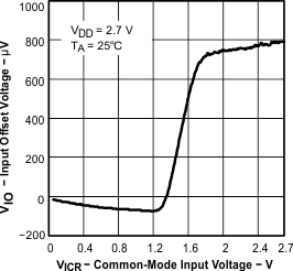 Figure 1. Input Offset Voltage
vs Common-Mode Input Voltage
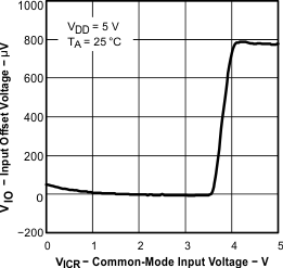 Figure 2. Input Offset Voltage
vs Common-Mode Input Voltage
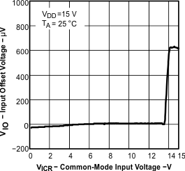 Figure 3. Input Offset Voltage
vs Common-Mode Input Voltage
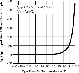 Figure 5. Input Bias and Offset Current
vs Free-Air Temperature
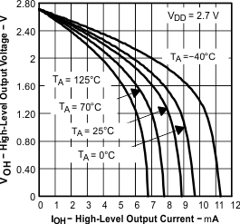 Figure 7. High-Level Output Voltage
vs High-Level Output Current
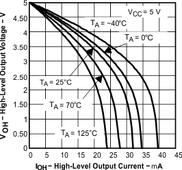 Figure 9. High-Level Output Voltage
vs High-Level Output Current
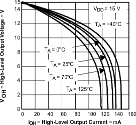 Figure 11. High-Level Output Voltage
vs High-Level Output Current
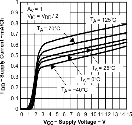 Figure 13. Supply Current vs Supply Voltage
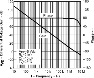 Figure 15. Differential Voltage Gain and Phase
vs Frequency
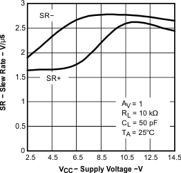 Figure 17. Slew Rate vs Supply Voltage
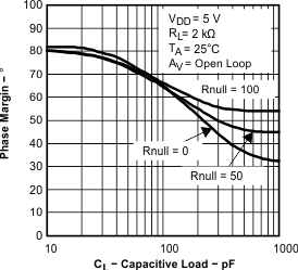 Figure 19. Phase Margin vs Capacitive Load
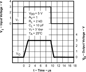 Figure 21. Voltage-Follower Large-Signal
Pulse Response
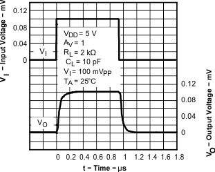 Figure 23. Voltage-Follower Small-Signal
Pulse Response
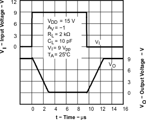 Figure 25. Inverting Large-Signal Response
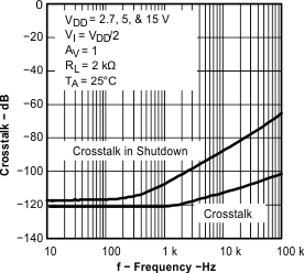 Figure 27. Crosstalk vs Frequency
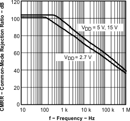 Figure 4. Common-Mode Rejection Ratio
vs Frequency
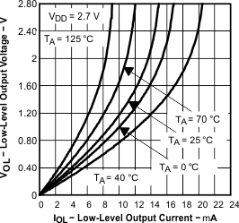 Figure 6. Low-Level Output Voltage
vs Low-Level Output Current
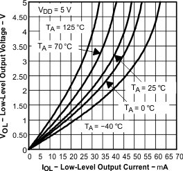 Figure 8. Low-Level Output Voltage
vs Low-Level Output Current
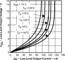 Figure 10. Low-Level Output Voltage
vs Low-Level Output Current
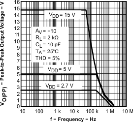 Figure 12. Peak-to-Peak Output Voltage
vs Frequency
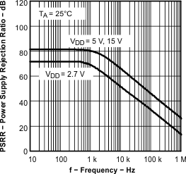 Figure 14. Power Supply Rejection Ratio
vs Frequency
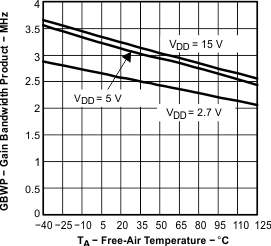 Figure 16. Gain Bandwidth Product
vs Free-Air Temperature
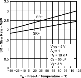 Figure 18. Slew Rate vs Free-Air Temperature
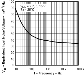 Figure 20. Equivalent Input Noise Voltage
vs Frequency
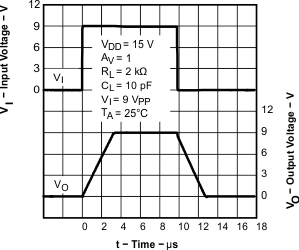 Figure 22. Voltage-Follower Large-Signal
Pulse Response
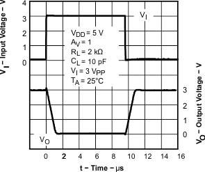 Figure 24. Inverting Large-Signal Response
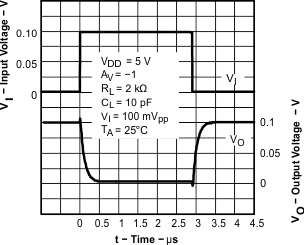 Figure 26. Inverting Small-Signal Response