JAJSBR5H February   2012  – June 2018 TLV62130 , TLV62130A

PRODUCTION DATA.  

  1. 特長
  2. アプリケーション
  3. 概要
    1.     Device Images
      1.      代表的なアプリケーションの回路図
      2.      効率と出力電流との関係
  4. 改訂履歴
  5. Device Comparison Table
  6. Pin Configuration and Functions
    1.     Pin Functions
  7. Specifications
    1. 7.1 Absolute Maximum Ratings
    2. 7.2 ESD Ratings
    3. 7.3 Recommended Operating Conditions
    4. 7.4 Thermal Information
    5. 7.5 Electrical Characteristics
    6. 7.6 Typical Characteristics
  8. Detailed Description
    1. 8.1 Overview
    2. 8.2 Functional Block Diagram
    3. 8.3 Feature Description
      1. 8.3.1 Enable / Shutdown (EN)
      2. 8.3.2 Soft Start / Tracking (SS/TR)
      3. 8.3.3 Power Good (PG)
      4. 8.3.4 Pin-Selectable Output Voltage (DEF)
      5. 8.3.5 Frequency Selection (FSW)
      6. 8.3.6 Undervoltage Lockout (UVLO)
      7. 8.3.7 Thermal Shutdown
    4. 8.4 Device Functional Modes
      1. 8.4.1 Pulse Width Modulation (PWM) Operation
      2. 8.4.2 Power Save Mode Operation
      3. 8.4.3 100% Duty-Cycle Operation
      4. 8.4.4 Current Limit and Short Circuit Protection
  9. Application and Implementation
    1. 9.1 Application Information
    2. 9.2 Typical Application
      1. 9.2.1 Design Requirements
      2. 9.2.2 Detailed Design Procedure
        1. 9.2.2.1 Custom Design With WEBENCH® Tools
        2. 9.2.2.2 Programming the Output Voltage
        3. 9.2.2.3 External Component Selection
          1. 9.2.2.3.1 Inductor Selection
          2. 9.2.2.3.2 Capacitor Selection
            1. 9.2.2.3.2.1 Output Capacitor
            2. 9.2.2.3.2.2 Input Capacitor
            3. 9.2.2.3.2.3 Soft Start Capacitor
        4. 9.2.2.4 Tracking Function
        5. 9.2.2.5 Output Filter and Loop Stability
      3. 9.2.3 Application Curves
    3. 9.3 System Examples
      1. 9.3.1 LED Power Supply
      2. 9.3.2 Active Output Discharge
      3. 9.3.3 Inverting Power Supply
      4. 9.3.4 Various Output Voltages
  10. 10Power Supply Recommendations
  11. 11Layout
    1. 11.1 Layout Guidelines
    2. 11.2 Layout Example
    3. 11.3 Thermal Considerations
  12. 12デバイスおよびドキュメントのサポート
    1. 12.1 デバイス・サポート
      1. 12.1.1 デベロッパー・ネットワークの製品に関する免責事項
      2. 12.1.2 開発サポート
        1. 12.1.2.1 WEBENCH®ツールによるカスタム設計
    2. 12.2 ドキュメントの更新通知を受け取る方法
    3. 12.3 ドキュメントのサポート
      1. 12.3.1 関連資料
    4. 12.4 関連リンク
    5. 12.5 コミュニティ・リソース
    6. 12.6 商標
    7. 12.7 静電気放電に関する注意事項
    8. 12.8 Glossary
  13. 13メカニカル、パッケージ、および注文情報

パッケージ・オプション

メカニカル・データ(パッケージ|ピン)
サーマルパッド・メカニカル・データ
発注情報

LED Power Supply

The TLV62130 can be used as a power supply for power LEDs. The FB pin can be easily set down to lower values than nominal by using the SS/TR pin. With that, the voltage drop on the sense resistor is low to avoid excessive power loss. Since this pin provides 2.5 µA, the feedback pin voltage can be adjusted by an external resistor per Equation 15. This drop, proportional to the LED current, is used to regulate the output voltage (anode voltage) to a proper level to drive the LED. Both analog and PWM dimming are supported with the TLV62130. Figure 38 shows an application circuit, tested with analog dimming:

spacing
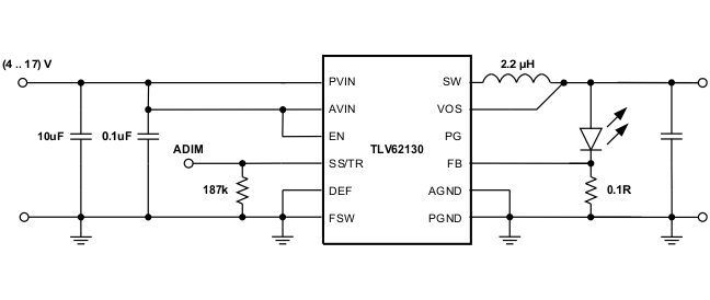
TLV62130 TLV62130A SLVSB74_LEDapp.gifFigure 38. 3 A Single LED Power Supply

spacing

The resistor at SS/TR sets the FB voltage to a level of about 300 mV and is calculated from Equation 15.

spacing

Equation 15. TLV62130 TLV62130A SLVSAG7_eqvfb.gif

spacing

The device now supplies a constant current, set by the resistor at the FB pin, by regulating the output voltage accordingly. The minimum input voltage has to be rated according the forward voltage needed by the LED used. More information is available in the Application Note SLVA451.

spacing