JAJSD06E December   2016  – April 2018 TLV8541 , TLV8542 , TLV8544

UNLESS OTHERWISE NOTED, this document contains PRODUCTION DATA.  

  1. 特長
  2. アプリケーション
  3. 概要
    1.     Device Images
      1.      低消費電力PIRモーション検出器
  4. 改訂履歴
  5. 概要(続き)
  6. Pin Configuration and Functions
    1.     Pin Functions: TLV8541 DBV
    2.     Pin Functions: TLV8542 D & RUG
    3.     Pin Functions: TLV8544 PW & D
  7. Specifications
    1. 7.1 Absolute Maximum Ratings
    2. 7.2 ESD Ratings
    3. 7.3 Recommended Operating Conditions
    4. 7.4 Thermal Information
    5. 7.5 Electrical Characteristics
    6. 7.6 Typical Characteristics
  8. Detailed Description
    1. 8.1 Overview
    2. 8.2 Functional Block Diagram
    3. 8.3 Feature Description
    4. 8.4 Device Functional Modes
      1. 8.4.1 Rail-To-Rail Input
      2. 8.4.2 Supply Current Changes Over Common Mode
      3. 8.4.3 Design Optimization With Rail-To-Rail Input
      4. 8.4.4 Design Optimization for Nanopower Operation
      5. 8.4.5 Common-Mode Rejection
      6. 8.4.6 Output Stage
      7. 8.4.7 Driving Capacitive Load
  9. Application and Implementation
    1. 9.1 Application Information
    2. 9.2 Typical Application: Battery-Powered Wireless PIR Motion Detectors
      1. 9.2.1 Design Requirements
      2. 9.2.2 Detailed Design Procedure
        1. 9.2.2.1 Calculation of the Cutoff Frequencies and Gain of Stage A:
        2. 9.2.2.2 Calculation of the Cutoff Frequencies and Gain of Stage B
        3. 9.2.2.3 Calculation of the Total Gain of Stages A and B
        4. 9.2.2.4 Window Comparator Stage
        5. 9.2.2.5 Reference Voltages
      3. 9.2.3 Application Curve
    3. 9.3 Typical Application: 60-Hz Twin T Notch Filter
      1. 9.3.1 Design Requirements
      2. 9.3.2 Detailed Design Procedure
      3. 9.3.3 Application Curve
    4. 9.4 Dos and Don'ts
  10. 10Power Supply Recommendations
  11. 11Layout
    1. 11.1 Layout Guidelines
    2. 11.2 Layout Example
  12. 12デバイスおよびドキュメントのサポート
    1. 12.1 デバイス・サポート
      1. 12.1.1 開発サポート
    2. 12.2 ドキュメントのサポート
      1. 12.2.1 関連資料
    3. 12.3 関連リンク
    4. 12.4 ドキュメントの更新通知を受け取る方法
    5. 12.5 コミュニティ・リソース
    6. 12.6 商標
    7. 12.7 静電気放電に関する注意事項
    8. 12.8 Glossary
  13. 13メカニカル、パッケージ、および注文情報

パッケージ・オプション

メカニカル・データ(パッケージ|ピン)
サーマルパッド・メカニカル・データ
発注情報

Application Curve

Scope plots of the amplified PIR signal at the input of the noninverting comparator and the corresponding output signal are shown in Figure 34 and Figure 35. As the PIR signal (blue line) crosses the VREF_High threshold, the output of the comparator switches from the cutoff (slightly higher than ground) state to the saturation state (slightly lower than VBAT = 3.3 V). Depending on the speed of the object, the PIR signal peaks to its maximum and roles off within several seconds. When the signal crosses the VREF_High threshold on the way down, the output of the noninverting amplifier toggles back to the cutoff region (low).

The data for plot of Figure 34 was captured using the BOOSTXL-TLV8544PIR board. Because the motion was created at very close proximity of the sensor on the booster board used to collect the data, the signal was limited by the diode in the first stage as shown in the plot.
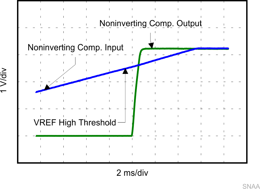
TLV8544 TLV8542 TLV8541 SNAA304_Noninverting_comp_scope-rev2.pngFigure 34. Noninverting Comparator Input and Output Signals

Referring to Figure 34, the output of the inverting comparator during the lower cycle of the PIR signal switches form the cutoff region to the saturation region as the input signal crosses the VREF_Low threshold.
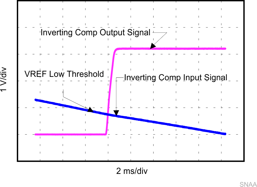
TLV8544 TLV8542 TLV8541 SNAA304_Inverting_comp_scope-rev2.pngFigure 35. Noninverting Comparator Input and Output Signals