JAJSGR1E October 2014 – September 2021 TMP102-Q1
PRODUCTION DATA
- 1 特長
- 2 アプリケーション
- 3 概要
- 4 Revision History
- 5 Pin Configuration and Functions
- 6 Specifications
-
7 Detailed Description
- 7.1 Overview
- 7.2 Functional Block Diagram
- 7.3
Feature Description
- 7.3.1 Digital Temperature Output
- 7.3.2 Serial Interface
- 7.3.3 Bus Overview
- 7.3.4 Serial Bus Address
- 7.3.5 Writing and Reading Operation
- 7.3.6 Slave Mode Operations
- 7.3.7 SMBus Alert Function
- 7.3.8 General Call
- 7.3.9 High-Speed (Hs) Mode
- 7.3.10 Time-Out Function
- 7.3.11 Timing Diagrams
- 7.3.12 Two-Wire Timing Diagrams
- 7.4 Device Functional Modes
- 7.5 Programming
- 8 Application and Implementation
- 9 Power Supply Recommendations
- 10Layout
- 11Device and Documentation Support
- 12Mechanical, Packaging, and Orderable Information
8.2.2 Detailed Design Procedure
Place the TMP102-Q1 device in close proximity to the heat source that must be monitored, with a proper layout for good thermal coupling. This placement ensures that temperature changes are captured within the shortest possible time interval. To maintain accuracy in applications that require air or surface temperature measurement, care must be taken to isolate the package and leads from ambient air temperature. A thermally-conductive adhesive is helpful in achieving accurate surface temperature measurement.
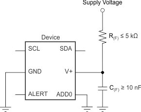
The TMP102-Q1 device is a very low-power device and generates very low noise on the supply bus. Applying an RC filter to the V+ pin of the TMP102-Q1 device can further reduce any noise that the TMP102-Q1 device might propagate to other components. R(F) in Figure 8-2 must be less than 5 kΩ and C(F) must be greater than 10 nF.
 Figure 8-2 Noise Reduction Techniques