JAJSGC5D February 2011 – December 2018 TMP103
PRODUCTION DATA.
- 1 特長
- 2 アプリケーション
- 3 概要
- 4 改訂履歴
- 5 Pin Configuration and Functions
- 6 Specifications
-
7 Detailed Description
- 7.1 Overview
- 7.2 Functional Block Diagram
- 7.3 Feature Description
- 7.4 Device Functional Modes
- 7.5
Programming
- 7.5.1 Temperature Watchdog Function
- 7.5.2 Conversion Rate
- 7.5.3 Shutdown Mode (M1 = 0, M0 = 0)
- 7.5.4 One-Shot (M1 = 0, M0 = 1)
- 7.5.5 Continuous Conversion Mode (M1 = 1)
- 7.5.6 Bus Overview
- 7.5.7 Serial Interface
- 7.5.8 Serial Bus Address
- 7.5.9 Writing and Reading Operation
- 7.5.10 Slave Mode Operations
- 7.5.11 General Call
- 7.5.12 High-Speed (Hs) Mode
- 7.5.13 Timeout Function
- 7.5.14 Multiple Device Access
- 7.5.15 NOISE
- 7.6 Register Maps
- 8 Application and Implementation
- 9 Power Supply Recommendations
- 10Layout
- 11デバイスおよびドキュメントのサポート
- 12メカニカル、パッケージ、および注文情報
パッケージ・オプション
デバイスごとのパッケージ図は、PDF版データシートをご参照ください。
メカニカル・データ(パッケージ|ピン)
- YFF|4
サーマルパッド・メカニカル・データ
発注情報
7.1 Overview
The TMP103 is a digital output temperature sensor in a wafer chip-scale package (WCSP) that is optimal for thermal management and thermal profiling. The TMP103 includes a two-wire interface that is compatible with both I2C and SMBus interfaces. In addition, the TMP103 has the capability of executing multiple device access (MDA) commands that allow multiple TMP103 devices to respond to a single global bus command. MDA commands reduce communication time and power in a bus that contains multiple TMP103 devices. The TMP103 is specified over a temperature range of –40ºC to 125ºC.
The TMP103 serial interface is designed to support up to eight TMP103 devices on a single bus. The TMP103 is offered with eight internal interface addresses. Each unique address option can be used as a location or temperature zone designator. The TMP103 responds to standard I2C and SMBus slave protocols that allow the internal registers to be written to or read from on an individual basis. The TMP103 also responds to MDA commands that allow all the devices on the bus to be written to or read from, without having to send the individual address and commands to each device.
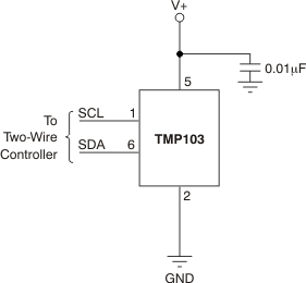
Pullup resistors are required on SCL and SDA. TI also recommends a 0.01-μF bypass capacitor, as shown in Figure 11.

The temperature sensor in the TMP103 is the chip itself. Thermal paths run through the package bumps as well as the package. The lower thermal resistance of metal causes the bumps to provide the primary thermal path.
To maintain accuracy in applications that require air or surface temperature measurement, take care to isolate the package from ambient air temperature.