JAJSHZ0A April   2013  – September 2019 TMP108

PRODUCTION DATA.  

  1. 特長
  2. アプリケーション
  3. 概要
    1.     Device Images
      1.      ブロック図
  4. 改訂履歴
  5. Pin Configuration and Functions
    1.     Pin Functions
  6. Specifications
    1. 6.1 Absolute Maximum Ratings
    2. 6.2 ESD Ratings
    3. 6.3 Recommended Operating Conditions
    4. 6.4 Thermal Information
    5. 6.5 Electrical Characteristics
    6. 6.6 Timing Diagrams
      1. 6.6.1 Two-Wire Timing Diagrams
    7. 6.7 Typical Characteristics
  7. Detailed Description
    1. 7.1 Overview
    2. 7.2 Functional Block Diagram
    3. 7.3 Feature Description
      1. 7.3.1 Serial Interface
      2. 7.3.2 Serial Bus Address
      3. 7.3.3 Bus Overview
      4. 7.3.4 Writing and Reading Operation
      5. 7.3.5 Slave Mode Operations
        1. 7.3.5.1 Slave Receiver Mode:
        2. 7.3.5.2 Slave Transmitter Mode:
      6. 7.3.6 SMBus Alert Function
      7. 7.3.7 General Call
      8. 7.3.8 High-Speed (Hs) Mode
      9. 7.3.9 Timeout Function
    4. 7.4 Device Functional Modes
      1. 7.4.1 Shutdown Mode (M1 = 0, M0 = 0)
      2. 7.4.2 One-Shot Mode (M1 = 0, M0 = 1)
      3. 7.4.3 Continuous Conversion Mode (M1 = 1)
    5. 7.5 Programming
      1. 7.5.1 Pointer Register
      2. 7.5.2 Temperature Register
      3. 7.5.3 Configuration Register
        1. 7.5.3.1 Hysteresis Control (HYS1 and HYS0)
        2. 7.5.3.2 Polarity (POL)
        3. 7.5.3.3 Thermostat Mode (TM)
        4. 7.5.3.4 Temperature Watchdog Flags (FL and FH)
        5. 7.5.3.5 Conversion Rate
      4. 7.5.4 High- and Low-Limit Registers
  8. Application and Implementation
    1. 8.1 Application Information
    2. 8.2 Typical Application
      1. 8.2.1 Design Requirements
      2. 8.2.2 Detailed Design Procedure
      3. 8.2.3 Application Curves
  9. Power Supply Recommendations
  10. 10Layout
    1. 10.1 Layout Guidelines
    2. 10.2 Layout Example
  11. 11デバイスおよびドキュメントのサポート
    1. 11.1 ドキュメントの更新通知を受け取る方法
    2. 11.2 サポート・リソース
    3. 11.3 商標
    4. 11.4 静電気放電に関する注意事項
    5. 11.5 Glossary
  12. 12メカニカル、パッケージ、および注文情報

パッケージ・オプション

メカニカル・データ(パッケージ|ピン)
サーマルパッド・メカニカル・データ
発注情報

Two-Wire Timing Diagrams

TMP108 ai_two_wire_tim_bos397.gifFigure 1. Two-Wire Timing Diagram
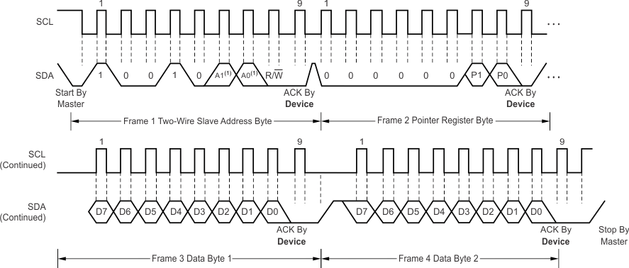
TMP108 ai_two_wire_write_bos663.gif
The value of A0 and A1 are determined by the A0 pin.
Figure 2. Two-Wire Timing Diagram for Write Word Format
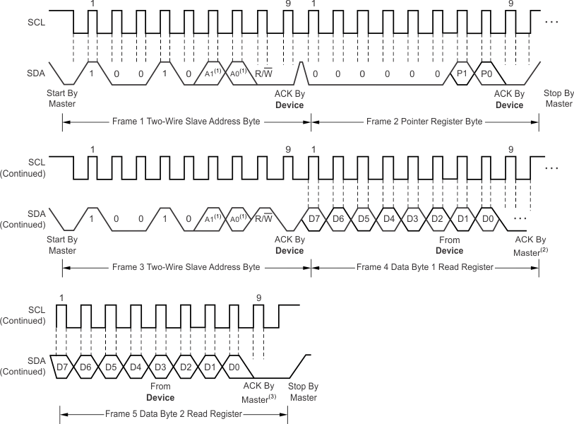
TMP108 ai_two_wire_read_bos663.gif
The value of A0 and A1 are determined by the A0 pin.
Master should leave SDA high to terminate a single-byte read operation.
Master should leave SDA high to terminate a two-byte read operation.
Figure 3. Two-Wire Timing Diagram for Read Word Format
TMP108 ai_tim_smbus_bos663.gif
The value of A0 and A1 are determined by the A0 pin.
Figure 4. Timing Diagram for SMBus Alert