JAJSFZ4E March 2009 – August 2018 TMS320C28341 , TMS320C28342 , TMS320C28343 , TMS320C28344 , TMS320C28345 , TMS320C28346
PRODUCTION DATA.
- 1デバイスの概要
- 2改訂履歴
- 3Device Comparison
- 4Terminal Configuration and Functions
-
5Specifications
- 5.1 Absolute Maximum Ratings
- 5.2 ESD Ratings – Automotive
- 5.3 ESD Ratings – Commercial
- 5.4 Recommended Operating Conditions
- 5.5 Power Consumption Summary
- 5.6 Electrical Characteristics
- 5.7 Thermal Resistance Characteristics
- 5.8 Thermal Design Considerations
- 5.9
Timing and Switching Characteristics
- 5.9.1 Timing Parameter Symbology
- 5.9.2 Power Sequencing
- 5.9.3 Clock Requirements and Characteristics
- 5.9.4
Peripherals
- 5.9.4.1 General-Purpose Input/Output (GPIO)
- 5.9.4.2 Enhanced Control Peripherals
- 5.9.4.3 External Interrupt Timing
- 5.9.4.4 I2C Electrical Specification and Timing
- 5.9.4.5 Serial Peripheral Interface (SPI) Timing
- 5.9.4.6
Multichannel Buffered Serial Port (McBSP) Timing
- 5.9.4.6.1 McBSP Transmit and Receive Timing
- 5.9.4.6.2
McBSP as SPI Master or Slave Timing
- Table 5-36 McBSP as SPI Master or Slave Timing Requirements (CLKSTP = 10b, CLKXP = 0)
- Table 5-37 McBSP as SPI Master or Slave Switching Characteristics (CLKSTP = 10b, CLKXP = 0)
- Table 5-38 McBSP as SPI Master or Slave Timing Requirements (CLKSTP = 11b, CLKXP = 0)
- Table 5-39 McBSP as SPI Master or Slave Switching Characteristics (CLKSTP = 11b, CLKXP = 0)
- Table 5-40 McBSP as SPI Master or Slave Timing Requirements (CLKSTP = 10b, CLKXP = 1)
- Table 5-41 McBSP as SPI Master or Slave Switching Characteristics (CLKSTP = 10b, CLKXP = 1)
- Table 5-42 McBSP as SPI Master or Slave Timing Requirements (CLKSTP = 11b, CLKXP = 1)
- Table 5-43 McBSP as SPI Master or Slave Switching Characteristics (CLKSTP = 11b, CLKXP = 1)
- 5.9.5 Emulator Connection Without Signal Buffering for the MCU
- 5.9.6
External Interface (XINTF) Timing
- 5.9.6.1 USEREADY = 0
- 5.9.6.2 Synchronous Mode (USEREADY = 1, READYMODE = 0)
- 5.9.6.3 Asynchronous Mode (USEREADY = 1, READYMODE = 1)
- 5.9.6.4 XINTF Signal Alignment to XCLKOUT
- 5.9.6.5 External Interface Read Timing
- 5.9.6.6 External Interface Write Timing
- 5.9.6.7
External Interface Ready-on-Read Timing With One External Wait State
- Table 5-49 External Interface Read Switching Characteristics (Ready-on-Read, One Wait State)
- Table 5-50 External Interface Read Timing Requirements (Ready-on-Read, One Wait State)
- Table 5-51 Synchronous XREADY Timing Requirements (Ready-on-Read, One Wait State)
- Table 5-52 Asynchronous XREADY Timing Requirements (Ready-on-Read, One Wait State)
- 5.9.6.8 External Interface Ready-on-Write Timing With One External Wait State
- 5.9.6.9 XHOLD and XHOLDA Timing
-
6Detailed Description
- 6.1
Brief Descriptions
- 6.1.1 C28x CPU
- 6.1.2 Memory Bus (Harvard Bus Architecture)
- 6.1.3 Peripheral Bus
- 6.1.4 Real-Time JTAG and Analysis
- 6.1.5 External Interface (XINTF)
- 6.1.6 M0, M1 SARAMs
- 6.1.7 L0, L1, L2, L3, L4, L5, L6, L7, H0, H1, H2, H3, H4, H5 SARAMs
- 6.1.8 Boot ROM
- 6.1.9 Security
- 6.1.10 Peripheral Interrupt Expansion (PIE) Block
- 6.1.11 External Interrupts (XINT1–XINT7, XNMI)
- 6.1.12 Oscillator and PLL
- 6.1.13 Watchdog
- 6.1.14 Peripheral Clocking
- 6.1.15 Low-Power Modes
- 6.1.16 Peripheral Frames 0, 1, 2, 3 (PFn)
- 6.1.17 General-Purpose Input/Output (GPIO) Multiplexer
- 6.1.18 32-Bit CPU-Timers (0, 1, 2)
- 6.1.19 Control Peripherals
- 6.1.20 Serial Port Peripherals
- 6.2
Peripherals
- 6.2.1 DMA Overview
- 6.2.2 32-Bit CPU-Timer 0, CPU-Timer 1, CPU-Timer 2
- 6.2.3 Enhanced PWM Modules
- 6.2.4 High-Resolution PWM (HRPWM)
- 6.2.5 Enhanced CAP Modules
- 6.2.6 Enhanced QEP Modules
- 6.2.7 External ADC Interface
- 6.2.8 Multichannel Buffered Serial Port (McBSP) Module
- 6.2.9 Enhanced Controller Area Network (eCAN) Modules (eCAN-A and eCAN-B)
- 6.2.10 Serial Communications Interface (SCI) Modules (SCI-A, SCI-B, SCI-C)
- 6.2.11 Serial Peripheral Interface (SPI) Module (SPI-A, SPI-D)
- 6.2.12 Inter-Integrated Circuit (I2C)
- 6.2.13 GPIO MUX
- 6.2.14 External Interface (XINTF)
- 6.3 Memory Maps
- 6.4 Register Map
- 6.5 Interrupts
- 6.6 System Control
- 6.7 Low-Power Modes Block
- 6.1
Brief Descriptions
- 7Applications, Implementation, and Layout
- 8デバイスおよびドキュメントのサポート
- 9メカニカル、パッケージ、および注文情報
パッケージ・オプション
デバイスごとのパッケージ図は、PDF版データシートをご参照ください。
メカニカル・データ(パッケージ|ピン)
- ZFE|256
サーマルパッド・メカニカル・データ
発注情報
5.5.1 Reducing Current Consumption
Methods of reducing current consumption include the following:
- Turn off the clock to any peripheral module that is not used in a given application because each peripheral unit has an individual clock-enable bit. Table 5-3 indicates the typical reduction in current consumption achieved by turning off the clocks.
- Use any one of the three low-power modes to reduce current even further.
- Turn off XCLKOUT, reducing IDDIO current consumption by 15 mA (typical).
- Disable the pullups on pins that assume an output function and on XINTF pins for significant savings in IDDIO.
NOTE
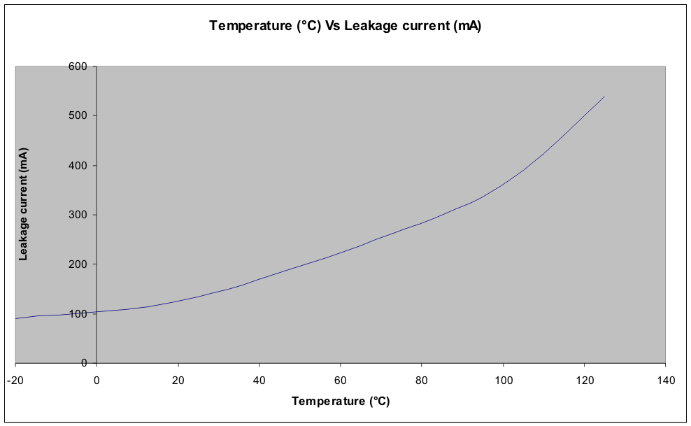
The TMS320C2834x devices are manufactured in a high-performance process node. Compared to the previous generation of the C28x devices, this process has more leakage current. Leakage current is significantly impacted by the operating temperature, and the increase in current with temperature is nonlinear. The total power for a given operating condition includes switching/active power plus leakage power. Low-power HALT mode power is due to the leakage current alone.
Figure 5-1 shows the typical leakage current across temperature.
 Figure 5-1 Temperature Versus Leakage Current (Typical)
 Table 5-3 Typical Current Consumption by Various Peripherals(1)
| PERIPHERAL
MODULE |
IDD CURRENT
REDUCTION (mA) |
|---|---|
| I2C | 5 |
| eQEP | 5 |
| ePWM | 3 |
| eCAP | 1 |
| SCI | 4 |
| SPI | 4 |
| eCAN | 2 |
| McBSP | 8 |
| CPU-Timer | 1 |
| XINTF | 4(2) |
| DMA | 7 |
| FPU | 8 |
- How many address/data pins toggle from one cycle to another
- How fast they toggle
- Whether 16-bit or 32-bit interface is used and
- The load on these pins.
- Whether internal pullups are enabled on the XINTF pins.