JAJSFZ4E March 2009 – August 2018 TMS320C28341 , TMS320C28342 , TMS320C28343 , TMS320C28344 , TMS320C28345 , TMS320C28346
PRODUCTION DATA.
- 1デバイスの概要
- 2改訂履歴
- 3Device Comparison
- 4Terminal Configuration and Functions
-
5Specifications
- 5.1 Absolute Maximum Ratings
- 5.2 ESD Ratings – Automotive
- 5.3 ESD Ratings – Commercial
- 5.4 Recommended Operating Conditions
- 5.5 Power Consumption Summary
- 5.6 Electrical Characteristics
- 5.7 Thermal Resistance Characteristics
- 5.8 Thermal Design Considerations
- 5.9
Timing and Switching Characteristics
- 5.9.1 Timing Parameter Symbology
- 5.9.2 Power Sequencing
- 5.9.3 Clock Requirements and Characteristics
- 5.9.4
Peripherals
- 5.9.4.1 General-Purpose Input/Output (GPIO)
- 5.9.4.2 Enhanced Control Peripherals
- 5.9.4.3 External Interrupt Timing
- 5.9.4.4 I2C Electrical Specification and Timing
- 5.9.4.5 Serial Peripheral Interface (SPI) Timing
- 5.9.4.6
Multichannel Buffered Serial Port (McBSP) Timing
- 5.9.4.6.1 McBSP Transmit and Receive Timing
- 5.9.4.6.2
McBSP as SPI Master or Slave Timing
- Table 5-36 McBSP as SPI Master or Slave Timing Requirements (CLKSTP = 10b, CLKXP = 0)
- Table 5-37 McBSP as SPI Master or Slave Switching Characteristics (CLKSTP = 10b, CLKXP = 0)
- Table 5-38 McBSP as SPI Master or Slave Timing Requirements (CLKSTP = 11b, CLKXP = 0)
- Table 5-39 McBSP as SPI Master or Slave Switching Characteristics (CLKSTP = 11b, CLKXP = 0)
- Table 5-40 McBSP as SPI Master or Slave Timing Requirements (CLKSTP = 10b, CLKXP = 1)
- Table 5-41 McBSP as SPI Master or Slave Switching Characteristics (CLKSTP = 10b, CLKXP = 1)
- Table 5-42 McBSP as SPI Master or Slave Timing Requirements (CLKSTP = 11b, CLKXP = 1)
- Table 5-43 McBSP as SPI Master or Slave Switching Characteristics (CLKSTP = 11b, CLKXP = 1)
- 5.9.5 Emulator Connection Without Signal Buffering for the MCU
- 5.9.6
External Interface (XINTF) Timing
- 5.9.6.1 USEREADY = 0
- 5.9.6.2 Synchronous Mode (USEREADY = 1, READYMODE = 0)
- 5.9.6.3 Asynchronous Mode (USEREADY = 1, READYMODE = 1)
- 5.9.6.4 XINTF Signal Alignment to XCLKOUT
- 5.9.6.5 External Interface Read Timing
- 5.9.6.6 External Interface Write Timing
- 5.9.6.7
External Interface Ready-on-Read Timing With One External Wait State
- Table 5-49 External Interface Read Switching Characteristics (Ready-on-Read, One Wait State)
- Table 5-50 External Interface Read Timing Requirements (Ready-on-Read, One Wait State)
- Table 5-51 Synchronous XREADY Timing Requirements (Ready-on-Read, One Wait State)
- Table 5-52 Asynchronous XREADY Timing Requirements (Ready-on-Read, One Wait State)
- 5.9.6.8 External Interface Ready-on-Write Timing With One External Wait State
- 5.9.6.9 XHOLD and XHOLDA Timing
-
6Detailed Description
- 6.1
Brief Descriptions
- 6.1.1 C28x CPU
- 6.1.2 Memory Bus (Harvard Bus Architecture)
- 6.1.3 Peripheral Bus
- 6.1.4 Real-Time JTAG and Analysis
- 6.1.5 External Interface (XINTF)
- 6.1.6 M0, M1 SARAMs
- 6.1.7 L0, L1, L2, L3, L4, L5, L6, L7, H0, H1, H2, H3, H4, H5 SARAMs
- 6.1.8 Boot ROM
- 6.1.9 Security
- 6.1.10 Peripheral Interrupt Expansion (PIE) Block
- 6.1.11 External Interrupts (XINT1–XINT7, XNMI)
- 6.1.12 Oscillator and PLL
- 6.1.13 Watchdog
- 6.1.14 Peripheral Clocking
- 6.1.15 Low-Power Modes
- 6.1.16 Peripheral Frames 0, 1, 2, 3 (PFn)
- 6.1.17 General-Purpose Input/Output (GPIO) Multiplexer
- 6.1.18 32-Bit CPU-Timers (0, 1, 2)
- 6.1.19 Control Peripherals
- 6.1.20 Serial Port Peripherals
- 6.2
Peripherals
- 6.2.1 DMA Overview
- 6.2.2 32-Bit CPU-Timer 0, CPU-Timer 1, CPU-Timer 2
- 6.2.3 Enhanced PWM Modules
- 6.2.4 High-Resolution PWM (HRPWM)
- 6.2.5 Enhanced CAP Modules
- 6.2.6 Enhanced QEP Modules
- 6.2.7 External ADC Interface
- 6.2.8 Multichannel Buffered Serial Port (McBSP) Module
- 6.2.9 Enhanced Controller Area Network (eCAN) Modules (eCAN-A and eCAN-B)
- 6.2.10 Serial Communications Interface (SCI) Modules (SCI-A, SCI-B, SCI-C)
- 6.2.11 Serial Peripheral Interface (SPI) Module (SPI-A, SPI-D)
- 6.2.12 Inter-Integrated Circuit (I2C)
- 6.2.13 GPIO MUX
- 6.2.14 External Interface (XINTF)
- 6.3 Memory Maps
- 6.4 Register Map
- 6.5 Interrupts
- 6.6 System Control
- 6.7 Low-Power Modes Block
- 6.1
Brief Descriptions
- 7Applications, Implementation, and Layout
- 8デバイスおよびドキュメントのサポート
- 9メカニカル、パッケージ、および注文情報
パッケージ・オプション
デバイスごとのパッケージ図は、PDF版データシートをご参照ください。
メカニカル・データ(パッケージ|ピン)
- ZFE|256
サーマルパッド・メカニカル・データ
発注情報
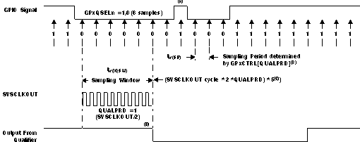
Table 5-11 General-Purpose Input Timing Requirements
| MIN | MAX | UNIT | |||
|---|---|---|---|---|---|
| tw(SP) | Sampling period | QUALPRD = 0 | 1tc(SCO) | cycles | |
| QUALPRD ≠ 0 | 2tc(SCO) * QUALPRD | ||||
| tw(IQSW) | Input qualifier sampling window | tw(SP) * (n(1) – 1) | cycles | ||
| tw(GPI)(2) | Pulse duration, GPIO low/high | Synchronous mode | 2tc(SCO) | cycles | |
| With input qualifier | tw(IQSW) + tw(SP) + 1tc(SCO) | ||||
(1) "n" represents the number of qualification samples as defined by GPxQSELn register.
(2) For tw(GPI), pulse width is measured from VIL to VIL for an active low signal and VIH to VIH for an active high signal.

A. This glitch will be ignored by the input qualifier. The QUALPRD bit field specifies the qualification sampling period. It can vary from 00 to 0xFF. If QUALPRD = 00, then the sampling period is 1 SYSCLKOUT cycle. For any other value "n", the qualification sampling period in 2n SYSCLKOUT cycles (that is, at every 2n SYSCLKOUT cycles, the GPIO pin will be sampled).
B. The qualification period selected through the GPxCTRL register applies to groups of 8 GPIO pins.
C. The qualification block can take either three or six samples. The GPxQSELn Register selects which sample mode is used.
D. In the example shown, for the qualifier to detect the change, the input should be stable for 10 SYSCLKOUT cycles or greater. In other words, the inputs should be stable for (5 × QUALPRD × 2) SYSCLKOUT cycles. This would ensure 5 sampling periods for detection to occur. Because external signals are driven asynchronously, an 13-SYSCLKOUT-wide pulse ensures reliable recognition.
Figure 5-8 Sampling Mode