JAJSFZ4E March 2009 – August 2018 TMS320C28341 , TMS320C28342 , TMS320C28343 , TMS320C28344 , TMS320C28345 , TMS320C28346
PRODUCTION DATA.
- 1デバイスの概要
- 2改訂履歴
- 3Device Comparison
- 4Terminal Configuration and Functions
-
5Specifications
- 5.1 Absolute Maximum Ratings
- 5.2 ESD Ratings – Automotive
- 5.3 ESD Ratings – Commercial
- 5.4 Recommended Operating Conditions
- 5.5 Power Consumption Summary
- 5.6 Electrical Characteristics
- 5.7 Thermal Resistance Characteristics
- 5.8 Thermal Design Considerations
- 5.9
Timing and Switching Characteristics
- 5.9.1 Timing Parameter Symbology
- 5.9.2 Power Sequencing
- 5.9.3 Clock Requirements and Characteristics
- 5.9.4
Peripherals
- 5.9.4.1 General-Purpose Input/Output (GPIO)
- 5.9.4.2 Enhanced Control Peripherals
- 5.9.4.3 External Interrupt Timing
- 5.9.4.4 I2C Electrical Specification and Timing
- 5.9.4.5 Serial Peripheral Interface (SPI) Timing
- 5.9.4.6
Multichannel Buffered Serial Port (McBSP) Timing
- 5.9.4.6.1 McBSP Transmit and Receive Timing
- 5.9.4.6.2
McBSP as SPI Master or Slave Timing
- Table 5-36 McBSP as SPI Master or Slave Timing Requirements (CLKSTP = 10b, CLKXP = 0)
- Table 5-37 McBSP as SPI Master or Slave Switching Characteristics (CLKSTP = 10b, CLKXP = 0)
- Table 5-38 McBSP as SPI Master or Slave Timing Requirements (CLKSTP = 11b, CLKXP = 0)
- Table 5-39 McBSP as SPI Master or Slave Switching Characteristics (CLKSTP = 11b, CLKXP = 0)
- Table 5-40 McBSP as SPI Master or Slave Timing Requirements (CLKSTP = 10b, CLKXP = 1)
- Table 5-41 McBSP as SPI Master or Slave Switching Characteristics (CLKSTP = 10b, CLKXP = 1)
- Table 5-42 McBSP as SPI Master or Slave Timing Requirements (CLKSTP = 11b, CLKXP = 1)
- Table 5-43 McBSP as SPI Master or Slave Switching Characteristics (CLKSTP = 11b, CLKXP = 1)
- 5.9.5 Emulator Connection Without Signal Buffering for the MCU
- 5.9.6
External Interface (XINTF) Timing
- 5.9.6.1 USEREADY = 0
- 5.9.6.2 Synchronous Mode (USEREADY = 1, READYMODE = 0)
- 5.9.6.3 Asynchronous Mode (USEREADY = 1, READYMODE = 1)
- 5.9.6.4 XINTF Signal Alignment to XCLKOUT
- 5.9.6.5 External Interface Read Timing
- 5.9.6.6 External Interface Write Timing
- 5.9.6.7
External Interface Ready-on-Read Timing With One External Wait State
- Table 5-49 External Interface Read Switching Characteristics (Ready-on-Read, One Wait State)
- Table 5-50 External Interface Read Timing Requirements (Ready-on-Read, One Wait State)
- Table 5-51 Synchronous XREADY Timing Requirements (Ready-on-Read, One Wait State)
- Table 5-52 Asynchronous XREADY Timing Requirements (Ready-on-Read, One Wait State)
- 5.9.6.8 External Interface Ready-on-Write Timing With One External Wait State
- 5.9.6.9 XHOLD and XHOLDA Timing
-
6Detailed Description
- 6.1
Brief Descriptions
- 6.1.1 C28x CPU
- 6.1.2 Memory Bus (Harvard Bus Architecture)
- 6.1.3 Peripheral Bus
- 6.1.4 Real-Time JTAG and Analysis
- 6.1.5 External Interface (XINTF)
- 6.1.6 M0, M1 SARAMs
- 6.1.7 L0, L1, L2, L3, L4, L5, L6, L7, H0, H1, H2, H3, H4, H5 SARAMs
- 6.1.8 Boot ROM
- 6.1.9 Security
- 6.1.10 Peripheral Interrupt Expansion (PIE) Block
- 6.1.11 External Interrupts (XINT1–XINT7, XNMI)
- 6.1.12 Oscillator and PLL
- 6.1.13 Watchdog
- 6.1.14 Peripheral Clocking
- 6.1.15 Low-Power Modes
- 6.1.16 Peripheral Frames 0, 1, 2, 3 (PFn)
- 6.1.17 General-Purpose Input/Output (GPIO) Multiplexer
- 6.1.18 32-Bit CPU-Timers (0, 1, 2)
- 6.1.19 Control Peripherals
- 6.1.20 Serial Port Peripherals
- 6.2
Peripherals
- 6.2.1 DMA Overview
- 6.2.2 32-Bit CPU-Timer 0, CPU-Timer 1, CPU-Timer 2
- 6.2.3 Enhanced PWM Modules
- 6.2.4 High-Resolution PWM (HRPWM)
- 6.2.5 Enhanced CAP Modules
- 6.2.6 Enhanced QEP Modules
- 6.2.7 External ADC Interface
- 6.2.8 Multichannel Buffered Serial Port (McBSP) Module
- 6.2.9 Enhanced Controller Area Network (eCAN) Modules (eCAN-A and eCAN-B)
- 6.2.10 Serial Communications Interface (SCI) Modules (SCI-A, SCI-B, SCI-C)
- 6.2.11 Serial Peripheral Interface (SPI) Module (SPI-A, SPI-D)
- 6.2.12 Inter-Integrated Circuit (I2C)
- 6.2.13 GPIO MUX
- 6.2.14 External Interface (XINTF)
- 6.3 Memory Maps
- 6.4 Register Map
- 6.5 Interrupts
- 6.6 System Control
- 6.7 Low-Power Modes Block
- 6.1
Brief Descriptions
- 7Applications, Implementation, and Layout
- 8デバイスおよびドキュメントのサポート
- 9メカニカル、パッケージ、および注文情報
パッケージ・オプション
デバイスごとのパッケージ図は、PDF版データシートをご参照ください。
メカニカル・データ(パッケージ|ピン)
- ZFE|256
サーマルパッド・メカニカル・データ
発注情報
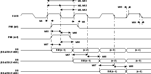
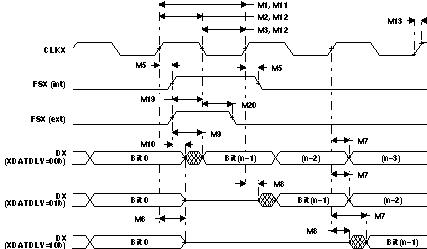
Table 5-35 McBSP Switching Characteristics(1)(2)
| NO. | PARAMETER | MIN | MAX | UNIT | |||
|---|---|---|---|---|---|---|---|
| M1 | tc(CKRX) | Cycle time, CLKR/X | CLKR/X int | 2P | ns | ||
| M2 | tw(CKRXH) | Pulse duration, CLKR/X high | CLKR/X int | D – 2 (3) | D + 2 (3) | ns | |
| M3 | tw(CKRXL) | Pulse duration, CLKR/X low | CLKR/X int | C – 2 (3) | C + 2 (3) | ns | |
| M4 | td(CKRH-FRV) | Delay time, CLKR high to internal FSR valid | CLKR int | 0 | 4 | ns | |
| CLKR ext | 3 | 20 | |||||
| M5 | td(CKXH-FXV) | Delay time, CLKX high to internal FSX valid | CLKX int | 0 | 4 | ns | |
| CLKX ext | 3 | 20 | |||||
| M6 | tdis(CKXH-DXHZ) | Disable time, CLKX high to DX high impedance following last data bit | CLKX int | 8 | ns | ||
| CLKX ext | 14 | ||||||
| M7 | td(CKXH-DXV) | Delay time, CLKX high to DX valid. | CLKX int | 4 | ns | ||
| This applies to all bits except the first bit transmitted. | CLKX ext | 20 | |||||
| Delay time, CLKX high to DX valid | DXENA = 0 | CLKX int | 4 | ||||
| CLKX ext | 20 | ||||||
| Only applies to first bit transmitted when in Data Delay 1 or 2 (XDATDLY=01b or 10b) modes | DXENA = 1 | CLKX int | P + 4 | ||||
| CLKX ext | P + 20 | ||||||
| M8 | ten(CKXH-DX) | Enable time, CLKX high to DX driven | DXENA = 0 | CLKX int | 0 | ns | |
| CLKX ext | 10 | ||||||
| Only applies to first bit transmitted when in Data Delay 1 or 2 (XDATDLY=01b or 10b) modes | DXENA = 1 | CLKX int | P | ||||
| CLKX ext | P + 10 | ||||||
| M9 | td(FXH-DXV) | Delay time, FSX high to DX valid | DXENA = 0 | FSX int | 4 | ns | |
| FSX ext | 16 | ||||||
| Only applies to first bit transmitted when in Data Delay 0 (XDATDLY=00b) mode. | DXENA = 1 | FSX int | P + 4 | ||||
| FSX ext | P + 16 | ||||||
| M10 | ten(FXH-DX) | Enable time, FSX high to DX driven | DXENA = 0 | FSX int | 0 | ns | |
| FSX ext | 6 | ||||||
| Only applies to first bit transmitted when in Data Delay 0 (XDATDLY=00b) mode | DXENA = 1 | FSX int | P | ||||
| FSX ext | P + 6 | ||||||
(1) Polarity bits CLKRP = CLKXP = FSRP = FSXP = 0. If the polarity of any of the signals is inverted, then the timing references of that signal are also inverted.
(2) 2P = 1/CLKG in ns.
(3) C = CLKRX low pulse width = P
D = CLKRX high pulse width = P
D = CLKRX high pulse width = P
 Figure 5-20 McBSP Receive Timing
  Figure 5-21 McBSP Transmit Timing