SPRS727C August 2012 – April 2014 TMS320C5517
PRODUCTION DATA.
- 1Device Overview
- 2Revision History
- 3Device Comparison
-
4Terminal Configuration and Functions
- 4.1 Pin Diagram
- 4.2
Signal Descriptions
- 4.2.1 Oscillator and PLL
- 4.2.2 Real-Time Clock (RTC)
- 4.2.3 RESET, Interrupts, and JTAG
- 4.2.4 External Memory Interface (EMIF)
- 4.2.5 Inter-Integrated Circuit (I2C)
- 4.2.6 Inter-IC Sound (I2S)
- 4.2.7 Multichannel Buffered Serial Port (McBSP)
- 4.2.8 Multichannel Serial Port Interface (McSPI)
- 4.2.9 Serial Peripheral Interface (SPI)
- 4.2.10 Universal Asynchronous Receiver and Transmitter (UART)
- 4.2.11 Universal Serial Bus (USB) 2.0
- 4.2.12 Universal Host-Port Interface (UHPI)
- 4.2.13 MultiMedia Card (MMC)
- 4.2.14 Successive Approximation (SAR) Analog-to-Digital Converter (ADC)
- 4.2.15 General-Purpose Input and Output (GPIO)
- 4.2.16 Regulators and Power Management
- 4.2.17 Supply Voltage
- 4.2.18 Ground
- 4.3
Pin Multiplexing
- 4.3.1 UHPI, SPI, UART, I2S2, I2S3, and GP[31:27, 20:12] Pin Multiplexing [EBSR.PPMODE Bits]
- 4.3.2 MMC1, McSPI, and GP[11:6] Pin Multiplexing [EBSR.SP1MODE Bits]
- 4.3.3 MMC0, I2S0, McBSP, and GP[5:0] Pin Multiplexing [EBSR.SP0MODE Bits]
- 4.3.4 EMIF EM_A[20:15] and GP[26:21] Pin Multiplexing [EBSR.Axx_MODE bits]
- 4.4 Connections for Unused Signals
-
5Specifications
- 5.1 Absolute Maximum Ratings
- 5.2 Recommended Operating Conditions
- 5.3 Electrical Characteristics
- 5.4 Handling Ratings
- 5.5 Thermal Characteristics
- 5.6 Power-On Hours
- 5.7
Timing and Switching Characteristics
- 5.7.1 Parameter Information
- 5.7.2 Power Supplies
- 5.7.3
Reset
- 5.7.3.1 Power-On Reset (POR) Circuits
- 5.7.3.2 Pin Behavior at Reset
- 5.7.3.3 Reset Electrical Data and Timing
- 5.7.3.4 Configurations at Reset
- 5.7.3.5
Configurations After Reset
- 5.7.3.5.1 External Bus Selection Register (EBSR)
- 5.7.3.5.2 LDO Control Register [7004h]
- 5.7.3.5.3 EMIF and USB System Control Registers (ESCR and USBSCR) [1C33h and 1C32h]
- 5.7.3.5.4 Peripheral Clock Gating Control Registers (PCGCR1 and PCGCR2) [1C02h and 1C03h]
- 5.7.3.5.5 Pullup and Pulldown Inhibit Registers (PUDINHIBR1, 2, 3, 4, 5, 6, and 7) [1C17h, 1C18h, 1C19h, 1C4Ch, 1C4Dh, 1C4Fh, and 1C50h, respectively]
- 5.7.3.5.6 Output Slew Rate Control Register (OSRCR) [1C16h]
- 5.7.4
Clock Specifications
- 5.7.4.1 Recommended Clock and Control Signal Transition Behavior
- 5.7.4.2 Clock Considerations
- 5.7.4.3 PLLs
- 5.7.4.4 Input and Output Clocks Electrical Data and Timing
- 5.7.4.5 Wake-up Events, Interrupts, and XF
- 5.7.5 Direct Memory Access (DMA) Controller
- 5.7.6 External Memory Interface (EMIF)
- 5.7.7 General-Purpose Input/Output (GPIO)
- 5.7.8 Inter-Integrated Circuit (I2C)
- 5.7.9 Inter-IC Sound (I2S)
- 5.7.10 Multichannel Serial Port Interface (McSPI)
- 5.7.11 Multichannel Buffered Serial Port (McBSP)
- 5.7.12 Multimedia Card and Secure Digital (eMMC, MMC, SD, and SDHC)
- 5.7.13 Real-Time Clock (RTC)
- 5.7.14 SAR ADC (10-Bit)
- 5.7.15 Serial Port Interface (SPI)
- 5.7.16 Timers
- 5.7.17 Universal Asynchronous Receiver and Transmitter (UART)
- 5.7.18 Universal Host-Port Interface (UHPI)
- 5.7.19 Universal Serial Bus (USB) 2.0 Controller
- 5.7.20 Emulation and Debug
- 5.7.21 IEEE 1149.1 JTAG
-
6Detailed Description
- 6.1 CPU
- 6.2
Memory
- 6.2.1 Internal Memory
- 6.2.2 External Memory
- 6.2.3 Memory Map
- 6.2.4
Register Map
- 6.2.4.1 DMA Peripheral Register Description
- 6.2.4.2 EMIF Peripheral Register Description
- 6.2.4.3 GPIO Peripheral Register Description
- 6.2.4.4 I2C Peripheral Register Description
- 6.2.4.5 I2S Peripheral Register Description
- 6.2.4.6 McBSP Peripheral Register Descriptions
- 6.2.4.7 McSPI Peripheral Register Descriptions
- 6.2.4.8 MMC and SD Peripheral Register Description
- 6.2.4.9 RTC Peripheral Register Description
- 6.2.4.10 SAR ADC Peripheral Register Description
- 6.2.4.11 SPI Peripheral Register Descriptions
- 6.2.4.12 System Registers
- 6.2.4.13 Timers Peripheral Register Description
- 6.2.4.14 UART Peripheral Register Description
- 6.2.4.15 UHPI Peripheral Register Descriptions
- 6.2.4.16 USB2.0 Peripheral Register Descriptions
- 6.3 Identification
- 6.4 Boot Modes
- 7Device and Documentation Support
- 8Mechanical Packaging and Orderable Information
パッケージ・オプション
デバイスごとのパッケージ図は、PDF版データシートをご参照ください。
メカニカル・データ(パッケージ|ピン)
- ZCH|196
サーマルパッド・メカニカル・データ
発注情報
6 Detailed Description
6.1 CPU
This fixed-point digital signal processor (DSP) is based on the C55x CPU 3.3 generation processor core. The C55x DSP architecture achieves high performance and low power through increased parallelism and total focus on power savings. The CPU supports an internal bus structure that is composed of one program bus, three data read buses (one 32-bit data read bus and two 16-bit data read buses), two 16-bit data write buses, and additional buses dedicated to peripheral and DMA activity. These buses provide the ability to perform up to four data reads and two data writes in a single cycle. Each DMA controller can perform one 32-bit data transfer per cycle, in parallel and independent of the CPU activity.
The C55x CPU provides two multiply-accumulate (MAC) units, each capable of 17-bit x 17-bit multiplication in a single cycle. A central 40-bit arithmetic and logic unit (ALU) is supported by an additional 16-bit ALU. Use of the ALUs is under instruction set control, providing the ability to optimize parallel activity and power consumption. These resources are managed in the Address Unit (AU) and Data Unit (DU) of the C55x CPU.
The C55x DSP generation supports a variable byte width instruction set for improved code density. The Instruction Unit (IU) performs 32-bit program fetches from internal or external memory, stores them in a 128-byte Instruction Buffer Queue, and queues instructions for the Program Unit (PU). The Program Unit decodes the instructions, directs tasks to AU and DU resources, and manages the fully protected pipeline. Predictive branching capability avoids pipeline flushes on execution of conditional instruction calls.
For more detailed information on the CPU, see the C55x CPU 3.0 CPU Reference Guide [literature number SWPU073].
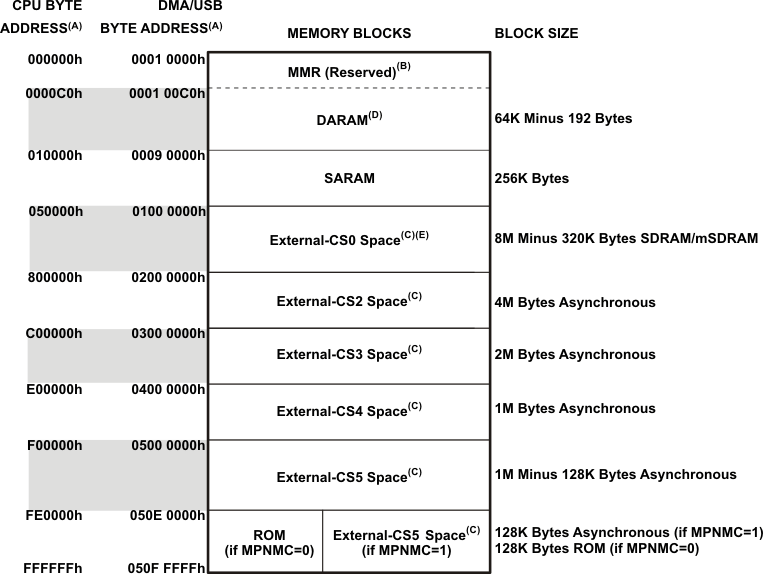
The C55x core of the device can address 16M bytes of unified data and program space. The core also addresses 64K words of I/O space and includes three types of on-chip memory: 128 KB read-only memory (ROM), 256 KB single-access random access memory (SARAM), 64 KB dual-access random access memory (DARAM). The memory map is shown in Figure 6-1.
6.2 Memory
6.2.1 Internal Memory
6.2.1.1 On-Chip Dual-Access RAM (DARAM)
The DARAM is located in the byte address range 000000h - 00FFFFh and is composed of eight blocks of 4K words each (see Table 6-1). Each DARAM block can support two accesses per cycle (two reads, two writes, or a read and a write). The DARAM can be accessed by the internal program, data, or DMA buses.
Table 6-1 DARAM Blocks
| CPU BYTE ADDRESS RANGE |
DMA CONTROLLER BYTE ADDRESS RANGE |
MEMORY BLOCK |
|---|---|---|
| 000000h – 001FFFh | 0001 0000h – 0001 1FFFh | DARAM 0(1) |
| 002000h – 003FFFh | 0001 2000h – 0001 3FFFh | DARAM 1 |
| 004000h – 005FFFh | 0001 4000h – 0001 5FFFh | DARAM 2 |
| 006000h – 007FFFh | 0001 6000h – 0001 7FFFh | DARAM 3 |
| 008000h – 009FFFh | 0001 8000h – 0001 9FFFh | DARAM 4 |
| 00A000h – 00BFFFh | 0001 A000h – 0001 BFFFh | DARAM 5 |
| 00C000h – 00DFFFh | 0001 C000h – 0001 DFFFh | DARAM 6 |
| 00E000h – 00FFFFh | 0001 E000h – 0001 FFFFh | DARAM 7 |
6.2.1.2 On-Chip Single-Access RAM (SARAM)
The SARAM is located at the byte address range 010000h – 04FFFFh and is composed of 32 blocks of 4K words each (see Table 6-2). Each SARAM block can support one access per cycle (one read or one write). SARAM can be accessed by the internal program, data, or DMA buses. SARAM is also accessed by the USB DMA buses.
Table 6-2 SARAM Blocks
| CPU BYTE ADDRESS RANGE |
DMA and USB CONTROLLER BYTE ADDRESS RANGE |
MEMORY BLOCK |
|---|---|---|
| 010000h - 011FFFh | 0009 0000h – 0009 1FFFh | SARAM 0 |
| 012000h - 013FFFh | 0009 2000h – 0009 3FFFh | SARAM 1 |
| 014000h - 015FFFh | 0009 4000h – 0009 5FFFh | SARAM 2 |
| 016000h - 017FFFh | 0009 6000h – 0009 7FFFh | SARAM 3 |
| 018000h - 019FFFh | 0009 8000h – 0009 9FFFh | SARAM 4 |
| 01A000h - 01BFFFh | 0009 A000h – 0009 BFFFh | SARAM 5 |
| 01C000h - 01DFFFh | 0009 C000h – 0009 DFFFh | SARAM 6 |
| 01E000h - 01FFFFh | 0009 E000h – 0009 FFFFh | SARAM 7 |
| 020000h - 021FFFh | 000A 0000h – 000A 1FFFh | SARAM 8 |
| 022000h - 023FFFh | 000A 2000h – 000A 3FFFh | SARAM 9 |
| 024000h - 025FFFh | 000A 4000h – 000A 5FFFh | SARAM 10 |
| 026000h - 027FFFh | 000A 6000h – 000A 7FFFh | SARAM 11 |
| 028000h - 029FFFh | 000A 8000h – 000A 9FFFh | SARAM 12 |
| 02A000h - 02BFFFh | 000A A000h – 000A BFFFh | SARAM 13 |
| 02C000h - 02DFFFh | 000A C000h – 000A DFFFh | SARAM 14 |
| 02E000h - 02FFFFh | 000A E000h – 000A FFFFh | SARAM 15 |
| 030000h - 031FFFh | 000B 0000h – 000B 1FFFh | SARAM 16 |
| 032000h - 033FFFh | 000B 2000h – 000B 3FFFh | SARAM 17 |
| 034000h - 035FFFh | 000B 4000h – 000B 5FFFh | SARAM 18 |
| 036000h - 037FFFh | 000B 6000h – 000B 7FFFh | SARAM 19 |
| 038000h - 039FFFh | 000B 8000h – 000B 9FFFh | SARAM 20 |
| 03A000h - 03BFFFh | 000B A000h – 000B BFFFh | SARAM 21 |
| 03C000h - 03DFFFh | 000B C000h – 000B DFFFh | SARAM 22 |
| 03E000h - 03FFFFh | 000B E000h – 000B FFFFh | SARAM 23 |
| 040000h – 041FFFh | 000C 0000h – 000C 1FFFh | SARAM 24 |
| 042000h – 043FFFh | 000C 2000h – 000C 3FFFh | SARAM 25 |
| 044000h – 045FFFh | 000C 4000h – 000C 5FFFh | SARAM 26 |
| 046000h – 047FFFh | 000C 6000h – 000C 7FFFh | SARAM 27 |
| 048000h – 049FFFh | 000C 8000h – 000C 9FFFh | SARAM 28 |
| 04A000h – 04BFFFh | 000C A000h – 000C BFFFh | SARAM 29 |
| 04C000h – 04DFFFh | 000C C000h – 000C DFFFh | SARAM 30 |
| 04E000h – 04FFFFh | 000C E000h – 000C FFFFh | SARAM 31(1) |
6.2.1.3 On-Chip Read-Only Memory (ROM)
The zero-wait-state ROM is located at the byte address range FE0000h – FFFFFFh. The ROM is composed of four 16K-word blocks, for a total of 128K bytes of ROM. Each on-chip ROM block can support one read per cycle. The ROM address space can be mapped by software to the EMIF external memory or to the internal ROM.
The standard device includes a Bootloader program resident in the ROM.
When the MPNMC bit field of the ST3 status register is cleared (by default), the byte address range FE0000h – FFFFFFh is used for the on-chip ROM. When the MPNMC bit field of the ST3 status register is set through software, the on-chip ROM is disabled and not present in the memory map, and byte address range FE0000h – FFFFFFh is directed to the EMIF's external memory space on EM_CS5. A hardware reset always clears the MPNMC bit, so it is not possible to disable the ROM at reset. However, the software reset instruction does not affect the MPNMC bit. The ROM can be accessed by the CPU program and data buses.
6.2.1.4 I/O Memory
The device includes a 64K byte I/O space for the memory-mapped registers of the DSP peripherals and system registers used for idle control, status monitoring and system configuration. I/O space is separate from program and memory space and is accessed with separate instruction opcodes or via the DMA's.
Table 6-3 lists the memory-mapped registers of the device. Note that not all addresses in the 64K byte I/O space are used; these addresses should be treated as RESERVED and not accessed by the CPU nor DMA. For the expanded tables of each peripheral, see Section 6.2.4, Register Map.
Some of the DMA controllers have access to the I/O-Space memory-mapped registers of the following peripherals registers: I2C, UART, I2S, MMC and SD, EMIF, McBSP, McSPI, USB, and SAR ADC.
Before accessing any peripheral memory-mapped register, make sure the peripheral being accessed is not held in reset via the Peripheral Reset Control Register (PRCR) and its internal clock is enabled via the Peripheral Clock Gating Control Registers (PCGCR1 and PCGCR2).
Table 6-3 Peripheral I/O-Space Control Registers
| WORD ADDRESS | PERIPHERAL |
|---|---|
| 0x0000 – 0x0004 | Idle Control |
| 0x0005 – 0x0BFF | Reserved |
| 0x0C00 – 0x0C7F | DMA0 |
| 0x0C80 – 0x0CFF | Reserved |
| 0x0D00 – 0x0D7F | DMA1 |
| 0x0D80 – 0x0DFF | Reserved |
| 0x0E00 – 0x0E7F | DMA2 |
| 0x0E80 – 0x0EFF | Reserved |
| 0x0F00 – 0x0F7F | DMA3 |
| 0x0F80 – 0x0FFF | Reserved |
| 0x1000 – 0x10DD | EMIF |
| 0x10DE – 0x17FF | Reserved |
| 0x1800 – 0x181F | Timer0 |
| 0x1820 – 0x183F | Reserved |
| 0x1840 – 0x185F | Timer1 |
| 0x1860 – 0x187F | Reserved |
| 0x1880 – 0x189F | Timer2 |
| 0x18A0 – 0x18FF | Reserved |
| 0x1900 – 0x197F | RTC |
| 0x1980 – 0x19FF | Reserved |
| 0x1A00 – 0x1A6C | I2C |
| 0x1A6D – 0x1AFF | Reserved |
| 0x1B00 – 0x1B1F | UART |
| 0x1B20 – 0x1BFF | Reserved |
| 0x1C00 – 0x1CFF | System Control |
| 0x1D00 – 0x1FFF through 0x2600 – 0x27FF | Reserved |
| 0x2800 – 0x2840 | I2S0 |
| 0x2841 – 0x29FF | Reserved |
| 0x2A00 – 0x2A40 | I2S2 |
| 0x2A41 – 0x2AFF | Reserved |
| 0x2B00 – 0x2B40 | I2S3 |
| 0x2B41 – 0x2DFF | Reserved |
| 0x2E00 – 0x2E81 | UHPI |
| 0x2E82 – 0x2FFF | Reserved |
| 0x3000 – 0x300F | SPI |
| 0x3010 – 0x33FF | Reserved |
| 0x3400 – 0x3749 | McSPI |
| 0x3750 –0x39FF | Reserved |
| 0x3A00 – 0x3A7F | MMC0 and SD0 |
| 0x3A80 – 0x3AFF | Reserved |
| 0x3B00 – 0x3B7F | MMC1 and SD1 |
| 0x3B80 – 0x3FFF | Reserved |
| 0x4000 – 0x407F | McBSP |
| 0x4080 – 0x5FFF | Reserved |
| 0x6000 – 0x60FF | McBSP DMA |
| 0x6100 – 0x6FFF | Reserved |
| 0x7000 – 0x70FF | SAR and Analog Control Registers |
| 0x7100 – 0x7FFF | Reserved |
| 0x8000 – 0xFFFF | USB |
6.2.2 External Memory
The external memory space of the device is located at the byte address range 050000h – FFFFFFh. The external memory space is divided into five chip select spaces: one dedicated to SDRAM and mobile SDRAM (EMIF CS0 or CS[1:0] space), and the remainder (EMIF CS2 through CS5 space) dedicated to asynchronous devices including flash. Each chip select space has a corresponding chip select pin (called EM_CSx) that is activated during an access to the chip select space.
The external memory interface (EMIF) provides the means for the DSP to access external memories and other devices including: mobile single data rate (SDR) synchronous dynamic RAM (SDRAM and mSDRAM), NOR Flash, NAND Flash, and asynchronous static RAM (SRAM). Before accessing external memory, you must configure the EMIF through its memory-mapped registers.
The EMIF provides a configurable 16- or 8-bit data bus, an address bus width of up to 21-bits, and 5 dedicated chip selects, along with memory control signals. To maximize power savings, the I/O pins of the EMIF can be operated at an independent voltage from the other I/O pins on the device.
6.2.3 Memory Map
The device provides 16M bytes of total memory space composed of on-chip RAM, on-chip ROM, and external memory space supporting a variety of memory types. The on-chip, dual-access RAM allows two accesses to a given block during the same cycle. There are 8 blocks of 8K bytes of dual-access RAM. The on-chip, single-access RAM allows one access to a given block per cycle. In addition, there are 32 blocks of 8K bytes of single-access RAM.
The remainder of the memory map is divided into five external spaces, and on-chip ROM. Each external space has a chip select decode signal (called EM_CS0, EM_CS[2:5]) that indicates an access to the selected space. The external memory interface (EMIF) supports access to asynchronous memories such as SRAM, NAND, or NOR and Flash, and mobile single data rate (mSDR) and single data rate (SDR) SDRAM.
The DSP memory is accessible by different master modules within the DSP, including the C55x CPU, the four DMA controllers, the UHPI, and the CDMA of USB (see Figure 6-1). However, only the UHPI and USB CDMA can access the SARAM.
6.2.4 Register Map
6.2.4.1 DMA Peripheral Register Description
The following tables show the registers associated with the four direct memory access (DMA) controllers.
Table 6-4 System Registers Related to the DMA Controllers
| CPU WORD ADDRESS | ACRONYM | REGISTER NAME |
|---|---|---|
| 1C30h | DMAIFR | DMA Interrupt Flag Register |
| 1C31h | DMAIER | DMA Interrupt Enable Register |
| 1C1Ah | DMA0CESRL | DMA0 Channel Event Source Register Lower |
| 1C1Bh | DMA0CESRU | DMA0 Channel Event Source Register Upper |
| 1C1Ch | DMA1CESRL | DMA1 Channel Event Source Register Lower |
| 1C1Dh | DMA1CESRU | DMA1 Channel Event Source Register Upper |
| 1C36h | DMA2CESRL | DMA2 Channel Event Source Register Lower |
| 1C37h | DMA2CESRU | DMA2 Channel Event Source Register Upper |
| 1C38h | DMA3CESRL | DMA3 Channel Event Source Register Lower |
| 1C39h | DMA3CESRU | DMA3 Channel Event Source Register Upper |
Table 6-5 DMA Controller 0 (DMA0) Registers
| CPU WORD ADDRESS | ACRONYM | REGISTER NAME |
|---|---|---|
| 0C00h | DMACH0SSAL | Channel 0 Source Start Address Register Lower |
| 0C01h | DMACH0SSAU | Channel 0 Source Start Address Register Upper |
| 0C02h | DMACH0DSAL | Channel 0 Destination Start Address Register Lower |
| 0C03h | DMACH0DSAU | Channel 0 Destination Start Address Register Upper |
| 0C04h | DMACH0TCRL | Channel 0 Transfer Control Register Lower |
| 0C05h | DMACH0TCRU | Channel 0 Transfer Control Register Upper |
| 0C20h | DMACH1SSAL | Channel 1 Source Start Address Register Lower |
| 0C21h | DMACH1SSAU | Channel 1 Source Start Address Register Upper |
| 0C22h | DMACH1DSAL | Channel 1 Destination Start Address Register Lower |
| 0C23h | DMACH1DSAU | Channel 1 Destination Start Address Register Upper |
| 0C24h | DMACH1TCRL | Channel 1 Transfer Control Register Lower |
| 0C25h | DMACH1TCRU | Channel 1 Transfer Control Register Upper |
| 0C40h | DMACH2SSAL | Channel 2 Source Start Address Register Lower |
| 0C41h | DMACH2SSAU | Channel 2 Source Start Address Register Upper |
| 0C42h | DMACH2DSAL | Channel 2 Destination Start Address Register Lower |
| 0C43h | DMACH2DSAU | Channel 2 Destination Start Address Register Upper |
| 0C44h | DMACH2TCRL | Channel 2 Transfer Control Register Lower |
| 0C45h | DMACH2TCRU | Channel 2 Transfer Control Register Upper |
| 0C60h | DMACH3SSAL | Channel 3 Source Start Address Register Lower |
| 0C61h | DMACH3SSAU | Channel 3 Source Start Address Register Upper |
| 0C62h | DMACH3DSAL | Channel 3 Destination Start Address Register Lower |
| 0C63h | DMACH3DSAU | Channel 3 Destination Start Address Register Upper |
| 0C64h | DMACH3TCRL | Channel 3 Transfer Control Register Lower |
| 0C65h | DMACH3TCRU | Channel 3 Transfer Control Register Upper |
Table 6-6 DMA Controller 1 (DMA1) Registers
| CPU WORD ADDRESS | ACRONYM | REGISTER NAME |
|---|---|---|
| 0D00h | DMACH0SSAL | Channel 0 Source Start Address Register Lower |
| 0D01h | DMACH0SSAU | Channel 0 Source Start Address Register Upper |
| 0D02h | DMACH0DSAL | Channel 0 Destination Start Address Register Lower |
| 0D03h | DMACH0DSAU | Channel 0 Destination Start Address Register Upper |
| 0D04h | DMACH0TCRL | Channel 0 Transfer Control Register Lower |
| 0D05h | DMACH0TCRU | Channel 0 Transfer Control Register Upper |
| 0D20h | DMACH1SSAL | Channel 1 Source Start Address Register Lower |
| 0D21h | DMACH1SSAU | Channel 1 Source Start Address Register Upper |
| 0D22h | DMACH1DSAL | Channel 1 Destination Start Address Register Lower |
| 0D23h | DMACH1DSAU | Channel 1 Destination Start Address Register Upper |
| 0D24h | DMACH1TCRL | Channel 1 Transfer Control Register Lower |
| 0D25h | DMACH1TCRU | Channel 1 Transfer Control Register Upper |
| 0D40h | DMACH2SSAL | Channel 2 Source Start Address Register Lower |
| 0D41h | DMACH2SSAU | Channel 2 Source Start Address Register Upper |
| 0D42h | DMACH2DSAL | Channel 2 Destination Start Address Register Lower |
| 0D43h | DMACH2DSAU | Channel 2 Destination Start Address Register Upper |
| 0D44h | DMACH2TCRL | Channel 2 Transfer Control Register Lower |
| 0D45h | DMACH2TCRU | Channel 2 Transfer Control Register Upper |
| 0D60h | DMACH3SSAL | Channel 3 Source Start Address Register Lower |
| 0D61h | DMACH3SSAU | Channel 3 Source Start Address Register Upper |
| 0D62h | DMACH3DSAL | Channel 3 Destination Start Address Register Lower |
| 0D63h | DMACH3DSAU | Channel 3 Destination Start Address Register Upper |
| 0D64h | DMACH3TCRL | Channel 3 Transfer Control Register Lower |
| 0D65h | DMACH3TCRU | Channel 3 Transfer Control Register Upper |
Table 6-7 DMA Controller 2 (DMA2) Registers
| CPU WORD ADDRESS | ACRONYM | REGISTER NAME |
|---|---|---|
| 0E00h | DMACH0SSAL | Channel 0 Source Start Address Register Lower |
| 0E01h | DMACH0SSAU | Channel 0 Source Start Address Register Upper |
| 0E02h | DMACH0DSAL | Channel 0 Destination Start Address Register Lower |
| 0E03h | DMACH0DSAU | Channel 0 Destination Start Address Register Upper |
| 0E04h | DMACH0TCRL | Channel 0 Transfer Control Register Lower |
| 0E05h | DMACH0TCRU | Channel 0 Transfer Control Register Upper |
| 0E20h | DMACH1SSAL | Channel 1 Source Start Address Register Lower |
| 0E21h | DMACH1SSAU | Channel 1 Source Start Address Register Upper |
| 0E22h | DMACH1DSAL | Channel 1 Destination Start Address Register Lower |
| 0E23h | DMACH1DSAU | Channel 1 Destination Start Address Register Upper |
| 0E24h | DMACH1TCRL | Channel 1 Transfer Control Register Lower |
| 0E25h | DMACH1TCRU | Channel 1 Transfer Control Register Upper |
| 0E40h | DMACH2SSAL | Channel 2 Source Start Address Register Lower |
| 0E41h | DMACH2SSAU | Channel 2 Source Start Address Register Upper |
| 0E42h | DMACH2DSAL | Channel 2 Destination Start Address Register Lower |
| 0E43h | DMACH2DSAU | Channel 2 Destination Start Address Register Upper |
| 0E44h | DMACH2TCRL | Channel 2 Transfer Control Register Lower |
| 0E45h | DMACH2TCRU | Channel 2 Transfer Control Register Upper |
| 0E60h | DMACH3SSAL | Channel 3 Source Start Address Register Lower |
| 0E61h | DMACH3SSAU | Channel 3 Source Start Address Register Upper |
| 0E62h | DMACH3DSAL | Channel 3 Destination Start Address Register Lower |
| 0E63h | DMACH3DSAU | Channel 3 Destination Start Address Register Upper |
| 0E64h | DMACH3TCRL | Channel 3 Transfer Control Register Lower |
| 0E65h | DMACH3TCRU | Channel 3 Transfer Control Register Upper |
Table 6-8 DMA Controller 3 (DMA3) Registers
| CPU WORD ADDRESS | ACRONYM | REGISTER NAME |
|---|---|---|
| 0F00h | DMACH0SSAL | Channel 0 Source Start Address Register Lower |
| 0F01h | DMACH0SSAU | Channel 0 Source Start Address Register Upper |
| 0F02h | DMACH0DSAL | Channel 0 Destination Start Address Register Lower |
| 0F03h | DMACH0DSAU | Channel 0 Destination Start Address Register Upper |
| 0F04h | DMACH0TCRL | Channel 0 Transfer Control Register Lower |
| 0F05h | DMACH0TCRU | Channel 0 Transfer Control Register Upper |
| 0F20h | DMACH1SSAL | Channel 1 Source Start Address Register Lower |
| 0F21h | DMACH1SSAU | Channel 1 Source Start Address Register Upper |
| 0F22h | DMACH1DSAL | Channel 1 Destination Start Address Register Lower |
| 0F23h | DMACH1DSAU | Channel 1 Destination Start Address Register Upper |
| 0F24h | DMACH1TCRL | Channel 1 Transfer Control Register Lower |
| 0F25h | DMACH1TCRU | Channel 1 Transfer Control Register Upper |
| 0F40h | DMACH2SSAL | Channel 2 Source Start Address Register Lower |
| 0F41h | DMACH2SSAU | Channel 2 Source Start Address Register Upper |
| 0F42h | DMACH2DSAL | Channel 2 Destination Start Address Register Lower |
| 0F43h | DMACH2DSAU | Channel 2 Destination Start Address Register Upper |
| 0F44h | DMACH2TCRL | Channel 2 Transfer Control Register Lower |
| 0F45h | DMACH2TCRU | Channel 2 Transfer Control Register Upper |
| 0F60h | DMACH3SSAL | Channel 3 Source Start Address Register Lower |
| 0F61h | DMACH3SSAU | Channel 3 Source Start Address Register Upper |
| 0F62h | DMACH3DSAL | Channel 3 Destination Start Address Register Lower |
| 0F63h | DMACH3DSAU | Channel 3 Destination Start Address Register Upper |
| 0F64h | DMACH3TCRL | Channel 3 Transfer Control Register Lower |
| 0F65h | DMACH3TCRU | Channel 3 Transfer Control Register Upper |
6.2.4.2 EMIF Peripheral Register Description
Table 6-9 shows the EMIF registers.
Table 6-9 External Memory Interface (EMIF) Peripheral Registers(1)
| CPU WORD ADDRESS | ACRONYM | REGISTER NAME |
|---|---|---|
| 1000h | REV | Revision Register |
| 1001h | STATUS | Status Register |
| 1004h | AWCCR1 | Asynchronous Wait Cycle Configuration Register 1 |
| 1005h | AWCCR2 | Asynchronous Wait Cycle Configuration Register 2 |
| 1008h | SDCR1 | SDRAM and mSDRAM Configuration Register 1 |
| 1009h | SDCR2 | SDRAM and mSDRAM Configuration Register 2 |
| 100Ch | SDRCR | SDRAM and mSDRAM Refresh Control Register |
| 1010h | ACS2CR1 | Asynchronous CS2 Configuration Register 1 |
| 1011h | ACS2CR2 | Asynchronous CS2 Configuration Register 2 |
| 1014h | ACS3CR1 | Asynchronous CS3 Configuration Register 1 |
| 1015h | ACS3CR2 | Asynchronous CS3 Configuration Register 2 |
| 1018h | ACS4CR1 | Asynchronous CS4 Configuration Register 1 |
| 1019h | ACS4CR2 | Asynchronous CS4 Configuration Register 2 |
| 101Ch | ACS5CR1 | Asynchronous CS5 Configuration Register 1 |
| 101Dh | ACS5CR2 | Asynchronous CS5 Configuration Register 2 |
| 1020h | SDTIMR1 | SDRAM and mSDRAM Timing Register 1 |
| 1021h | SDTIMR2 | SDRAM and mSDRAM Timing Register 2 |
| 103Ch | SDSRETR | SDRAM and mSDRAM Self Refresh Exit Timing Register |
| 1040h | EIRR | EMIF Interrupt Raw Register |
| 1044h | EIMR | EMIF Interrupt Mask Register |
| 1048h | EIMSR | EMIF Interrupt Mask Set Register |
| 104Ch | EIMCR | EMIF Interrupt Mask Clear Register |
| 1060h | NANDFCR | NAND Flash Control Register |
| 1064h | NANDFSR1 | NAND Flash Status Register 1 |
| 1065h | NANDFSR2 | NAND Flash Status Register 2 |
| 1068h | PAGEMODCTRL1 | Page Mode Control Register 1 |
| 1069h | PAGEMODCTRL2 | Page Mode Control Register 2 |
| 1070h | NCS2ECC1 | NAND Flash CS2 1-Bit ECC Register 1 |
| 1071h | NCS2ECC2 | NAND Flash CS2 1-Bit ECC Register 2 |
| 1074h | NCS3ECC1 | NAND Flash CS3 1-Bit ECC Register 1 |
| 1075h | NCS3ECC2 | NAND Flash CS3 1-Bit ECC Register 2 |
| 1078h | NCS4ECC1 | NAND Flash CS4 1-Bit ECC Register 1 |
| 1079h | NCS4ECC2 | NAND Flash CS4 1-Bit ECC Register 2 |
| 107Ch | NCS5ECC1 | NAND Flash CS5 1-Bit ECC Register 1 |
| 107Dh | NCS5ECC2 | NAND Flash CS5 1-Bit ECC Register 2 |
| 10BCh | NAND4BITECCLOAD | NAND Flash 4-Bit ECC Load Register |
| 10C0h | NAND4BITECC1 | NAND Flash 4-Bit ECC Register 1 |
| 10C1h | NAND4BITECC2 | NAND Flash 4-Bit ECC Register 2 |
| 10C4h | NAND4BITECC3 | NAND Flash 4-Bit ECC Register 3 |
| 10C5h | NAND4BITECC4 | NAND Flash 4-Bit ECC Register 4 |
| 10C8h | NAND4BITECC5 | NAND Flash 4-Bit ECC Register 5 |
| 10C9h | NAND4BITECC6 | NAND Flash 4-Bit ECC Register 6 |
| 10CCh | NAND4BITECC7 | NAND Flash 4-Bit ECC Register 7 |
| 10CDh | NAND4BITECC8 | NAND Flash 4-Bit ECC Register 8 |
| 10D0h | NANDERRADD1 | NAND Flash 4-Bit ECC Error Address Register 1 |
| 10D1h | NANDERRADD2 | NAND Flash 4-Bit ECC Error Address Register 2 |
| 10D4h | NANDERRADD3 | NAND Flash 4-Bit ECC Error Address Register 3 |
| 10D5h | NANDERRADD4 | NAND Flash 4-Bit ECC Error Address Register 4 |
| 10D8h | NANDERRVAL1 | NAND Flash 4-Bit ECC Error Value Register 1 |
| 10D9h | NANDERRVAL2 | NAND Flash 4-Bit ECC Error Value Register 2 |
| 10DCh | NANDERRVAL3 | NAND Flash 4-Bit ECC Error Value Register 3 |
| 10DDh | NANDERRVAL4 | NAND Flash 4-Bit ECC Error Value Register 4 |
6.2.4.3 GPIO Peripheral Register Description
The external parallel port interface includes a 16-bit general purpose I/O that can be individually programmed as input or output with interrupt capability. Control of the general purpose I/O is maintained through a set of I/O memory-mapped registers shown in Table 6-10.
Table 6-10 GPIO Registers
| CPU WORD ADDRESS | ACRONYM | REGISTER NAME |
|---|---|---|
| 1C06h | IODIR1 | GPIO Direction Register 1 |
| 1C07h | IODIR2 | GPIO Direction Register 2 |
| 1C08h | IOINDATA1 | GPIO Data In Register 1 |
| 1C09h | IOINDATA2 | GPIO Data In Register 2 |
| 1C0Ah | IODATAOUT1 | GPIO Data Out Register 1 |
| 1C0Bh | IODATAOUT2 | GPIO Data Out Register 2 |
| 1C0Ch | IOINTEDG1 | GPIO Interrupt Edge Trigger Enable Register 1 |
| 1C0Dh | IOINTEDG2 | GPIO Interrupt Edge Trigger Enable Register 2 |
| 1C0Eh | IOINTEN1 | GPIO Interrupt Enable Register 1 |
| 1C0Fh | IOINTEN2 | GPIO Interrupt Enable Register 2 |
| 1C10h | IOINTFLG1 | GPIO Interrupt Flag Register 1 |
| 1C11h | IOINTFLG2 | GPIO Interrupt Flag Register 2 |
6.2.4.4 I2C Peripheral Register Description
Table 6-11 shows the Inter-Integrated Circuit (I2C) registers.
Table 6-11 Inter-Integrated Circuit (I2C) Registers
| CPU WORD ADDRESS | ACRONYM | REGISTER NAME |
|---|---|---|
| 1A00h | ICOAR | I2C Own Address Register |
| 1A04h | ICIMR | I2C Interrupt Mask Register |
| 1A08h | ICSTR | I2C Interrupt Status Register |
| 1A0Ch | ICCLKL | I2C Clock Low-Time Divider Register |
| 1A10h | ICCLKH | I2C Clock High-Time Divider Register |
| 1A14h | ICCNT | I2C Data Count Register |
| 1A18h | ICDRR | I2C Data Receive Register |
| 1A1Ch | ICSAR | I2C Slave Address Register |
| 1A20h | ICDXR | I2C Data Transmit Register |
| 1A24h | ICMDR | I2C Mode Register |
| 1A28h | ICIVR | I2C Interrupt Vector Register |
| 1A2Ch | ICEMDR | I2C Extended Mode Register |
| 1A30h | ICPSC | I2C Prescaler Register |
| 1A34h | ICPID1 | I2C Peripheral Identification Register 1 |
| 1A38h | ICPID2 | I2C Peripheral Identification Register 2 |
6.2.4.5 I2S Peripheral Register Description
Table 6-12 through Table 6-14 show the I2S0, I2S2, and I2S3 registers.
Table 6-12 I2S0 Registers
| CPU WORD ADDRESS | ACRONYM | REGISTER NAME |
|---|---|---|
| 2800h | I2S0SCTRL | I2S0 Serializer Control Register |
| 2804h | I2S0SRATE | I2S0 Sample Rate Generator Register |
| 2808h | I2S0TXLT1 | I2S0 Transmit Left Data Register 1 |
| 2809h | I2S0TXLT2 | I2S0 Transmit Left Data Register 2 |
| 280Ch | I2S0TXRT1 | I2S0 Transmit Right Data Register 1 |
| 280Dh | I2S0TXRT2 | I2S0 Transmit Right Data Register 2 |
| 2810h | I2S0INTFL | I2S0 Interrupt Flag Register |
| 2814h | I2S0INTMASK | I2S0 Interrupt Mask Register |
| 2828h | I2S0RXLT1 | I2S0 Receive Left Data Register 1 |
| 2829h | I2S0RXLT2 | I2S0 Receive Left Data Register 2 |
| 282Ch | I2S0RXRT1 | I2S0 Receive Right Data Register 1 |
| 282Dh | I2S0RXRT2 | I2S0 Receive Right Data Register 2 |
Table 6-13 I2S2 Registers
| CPU WORD ADDRESS | ACRONYM | REGISTER NAME |
|---|---|---|
| 2A00h | I2S2SCTRL | I2S2 Serializer Control Register |
| 2A04h | I2S2SRATE | I2S2 Sample Rate Generator Register |
| 2A08h | I2S2TXLT1 | I2S2 Transmit Left Data Register 1 |
| 2A09h | I2S2TXLT2 | I2S2 Transmit Left Data Register 2 |
| 2A0Ch | I2S2TXRT1 | I2S2 Transmit Right Data Register 1 |
| 2A0Dh | I2S2TXRT2 | I2S2 Transmit Right Data Register 2 |
| 2A10h | I2S2INTFL | I2S2 Interrupt Flag Register |
| 2A14h | I2S2INTMASK | I2S2 Interrupt Mask Register |
| 2A28h | I2S2RXLT1 | I2S2 Receive Left Data Register 1 |
| 2A29h | I2S2RXLT2 | I2S2 Receive Left Data Register 2 |
| 2A2Ch | I2S2RXRT1 | I2S2 Receive Right Data Register 1 |
| 2A2Dh | I2S2RXRT2 | I2S2 Receive Right Data Register 2 |
Table 6-14 I2S3 Registers
| CPU WORD ADDRESS | ACRONYM | REGISTER NAME |
|---|---|---|
| 2B00h | I2S3SCTRL | I2S3 Serializer Control Register |
| 2B04h | I2S3SRATE | I2S3 Sample Rate Generator Register |
| 2B08h | I2S3TXLT1 | I2S3 Transmit Left Data Register 1 |
| 2B09h | I2S3TXLT2 | I2S3 Transmit Left Data Register 2 |
| 2B0Ch | I2S3TXRT1 | I2S3 Transmit Right Data Register 1 |
| 2B0Dh | I2S3TXRT2 | I2S3 Transmit Right Data Register 2 |
| 2B10h | I2S3INTFL | I2S3 Interrupt Flag Register |
| 2B14h | I2S3INTMASK | I2S3 Interrupt Mask Register |
| 2B28h | I2S3RXLT1 | I2S3 Receive Left Data Register 1 |
| 2B29h | I2S3RXLT2 | I2S3 Receive Left Data Register 2 |
| 2B2Ch | I2S3RXRT1 | I2S3 Receive Right Data Register 1 |
| 2B2Dh | I2S3RXRT2 | I2S3 Receive Right Data Register 2 |
6.2.4.6 McBSP Peripheral Register Descriptions
Table 6-15 shows the McBSP peripheral registers.
Table 6-15 McBSP Module Registers
| CPU WORD ADDRESS | ACRONYM | REGISTER NAME |
|---|---|---|
| 4000h | DRRL | Data Receive Register Lower |
| 4001h | DRRU | Data Receive Register Upper |
| 4004h | DXRL | Data Transmit Register Lower |
| 4005h | DXRU | Data Transmit Register Upper |
| 4008h | SPCRL | Serial Port Control Register Lower |
| 4009h | SPCRU | Serial Port Control Register Upper |
| 400Ch | RCRL | Receive Control Register Lower |
| 400Dh | RCRU | Receive Control Register Upper |
| 4010h | XCRL | Transmit Control Register Lower |
| 4011h | XCRU | Transmit Control Register Upper |
| 4014h | SRGRL | Sample Rate Generator Register Lower |
| 4015h | SRGRU | Sample Rate Generator Register Upper |
| 4018h | MCRL | Multichannel Control Register Lower |
| 4019h | MCRU | Multichannel Control Register Upper |
| 401Ch | RCERA | Enhanced Receive Channel Enable Register Partition A |
| 401Dh | RCERB | Enhanced Receive Channel Enable Register Partition B |
| 4020h | XCERA | Enhanced Transmit Channel Enable Register Partition A |
| 4021h | XCERB | Enhanced Transmit Channel Enable Register Partition B |
| 4024h | PCRL | Pin Control Register Lower |
| 4025h | PCRU | Pin Control Register Upper |
| 4028h | RCERC | Enhanced Receive Channel Enable Register Partition C |
| 4029h | RCERD | Enhanced Receive Channel Enable Register Partition D |
| 402Ch | XCERC | Enhanced Transmit Channel Enable Register Partition C |
| 402Dh | XCERD | Enhanced Transmit Channel Enable Register Partition D |
| 4030h | RCERE | Enhanced Receive Channel Enable Register Partition E |
| 4031h | RCERF | Enhanced Receive Channel Enable Register Partition F |
| 4034h | XCERE | Enhanced Transmit Channel Enable Register Partition E |
| 4035h | XCERF | Enhanced Transmit Channel Enable Register Partition F |
| 4038h | RCERG | Enhanced Receive Channel Enable Register Partition G |
| 4039h | RCERH | Enhanced Receive Channel Enable Register Partition H |
| 403Ch | XCERG | Enhanced Transmit Channel Enable Register Partition G |
| 403Dh | XCERH | Enhanced Transmit Channel Enable Register Partition H |
6.2.4.7 McSPI Peripheral Register Descriptions
Table 6-16 shows the McSPI peripheral registers.
Table 6-16 McSPI Module Registers
| CPU WORD ADDRESS | ACRONYM | REGISTER NAME |
|---|---|---|
| 3500h | REVISIONL | Revision Register Lower |
| 3510h | SYSCONFIGL | System Configuration Register Lower |
| 3514h | SYSSTATUSL | System Status Register Lower |
| 3518h | IRQSTATUSL | Interrupt Status Register Lower |
| 3519h | IRQSTATUSU | Interrupt Status Register Upper |
| 351Ch | IRQENABLEL | Interrupt Enable Register Lower |
| 351Dh | IRQENABLEU | Interrupt Enable Register Upper |
| 3520h | WAKEUPENABLEL | Wakeup Enable Register Lower |
| 3528h | MODULCTRLL | Module Control Register Lower |
| 352Ch | CH0CONFL | Channel 0 Configuration Register Lower |
| 352Dh | CH0CONFU | Channel 0 Configuration Register Upper |
| 3530h | CH0STATL | Channel 0 Status Register Lower |
| 3534h | CH0CTRLL | Channel 0 Control Register Lower |
| 3538h | CH0TXL | Channel 0 Transmitter Register Lower |
| 3539h | CH0TXU | Channel 0 Transmitter Register Upper |
| 353Ch | CH0RXL | Channel 0 Receiver Register Lower |
| 353Dh | CH0RXU | Channel 0 Receiver Register Upper |
| 3540h | CH1CONFL | Channel 1 Configuration Register Lower |
| 3541h | CH1CONFU | Channel 1 Configuration Register Upper |
| 3544h | CH1STATL | Channel 1 Status Register Lower |
| 3548h | CH1CTRLL | Channel 1 Control Register Lower |
| 354Ch | CH1TXL | Channel 1 Transmitter Register Lower |
| 354Dh | CH1TXU | Channel 1 Transmitter Register Upper |
| 3550h | CH1RXL | Channel 1 Receiver Register Lower |
| 3551h | CH1RXU | Channel 1 Receiver Register Upper |
| 3554h | CH2CONFL | Channel 2 Configuration Register Lower |
| 3555h | CH2CONFU | Channel 2 Configuration Register Upper |
| 3558h | CH2STATL | Channel 2 Status Register Lower |
| 355Ch | CH2CTRLL | Channel 2 Control Register Lower |
| 3560h | CH2TXL | Channel 2 Transmitter Register Lower |
| 3561h | CH2TXU | Channel 2 Transmitter Register Upper |
| 3564h | CH2RXL | Channel 2 Receiver Register Lower |
| 3565h | CH2RXU | Channel 2 Receiver Register Upper |
| 357Ch | XFERLEVELL | Transfer Levels Register Lower |
| 357Dh | XFERLEVELU | Transfer Levels Register Upper |
| 3580h | DAFTXL | DMA Address Aligned FIFO Transmitter Register Lower |
| 3581h | DAFTXU | DMA Address Aligned FIFO Transmitter Register Upper |
| 35A0h | DAFRXL | DMA Address Aligned FIFO Receiver Register Lower |
| 35A1h | DAFRXU | DMA Address Aligned FIFO Receiver Register Upper |
6.2.4.8 MMC and SD Peripheral Register Description
Table 6-17 and Table 6-18 show the MMC and SD registers. The MMC0 and SD0 registers start at address 0x3A00 and the MMC1 and SD1 registers start at address 0x3B00.
Table 6-17 MMC0 and SD0 Registers
| CPU WORD ADDRESS | ACRONYM | REGISTER NAME |
|---|---|---|
| 3A00h | MMCCTL | MMC Control Register |
| 3A04h | MMCCLK | MMC Memory Clock Control Register |
| 3A08h | MMCST0 | MMC Status Register 0 |
| 3A0Ch | MMCST1 | MMC Status Register 1 |
| 3A10h | MMCIM | MMC Interrupt Mask Register |
| 3A14h | MMCTOR | MMC Response Time-Out Register |
| 3A18h | MMCTOD | MMC Data Read Time-Out Register |
| 3A1Ch | MMCBLEN | MMC Block Length Register |
| 3A20h | MMCNBLK | MMC Number of Blocks Register |
| 3A24h | MMCNBLC | MMC Number of Blocks Counter Register |
| 3A28h | MMCDRRL | MMC Data Receive Register Lower |
| 3A29h | MMCDRRU | MMC Data Receive Register Upper |
| 3A2Ch | MMCDXRL | MMC Data Transmit Register Lower |
| 3A2Dh | MMCDXRU | MMC Data Transmit Register Upper |
| 3A30h | MMCCMDL | MMC Command Register Lower |
| 3A31h | MMCCMDU | MMC Command Register Upper |
| 3A34h | MMCARGL | MMC Argument Register Lower |
| 3A35h | MMCARGU | MMC Argument Register Upper |
| 3A38h | MMCRSP0 | MMC Response Register 0 |
| 3A39h | MMCRSP1 | MMC Response Register 1 |
| 3A3Ch | MMCRSP2 | MMC Response Register 2 |
| 3A3Dh | MMCRSP3 | MMC Response Register 3 |
| 3A40h | MMCRSP4 | MMC Response Register 4 |
| 3A41h | MMCRSP5 | MMC Response Register 5 |
| 3A44h | MMCRSP6 | MMC Response Register 6 |
| 3A45h | MMCRSP7 | MMC Response Register 7 |
| 3A48h | MMCDRSP | MMC Data Response Register |
| 3A50h | MMCCIDX | MMC Command Index Register |
| 3A64h | SDIOCTL | SDIO Control Register |
| 3A68h | SDIOST0 | SDIO Status Register 0 |
| 3A6Ch | SDIOIEN | SDIO Interrupt Enable Register |
| 3A70h | SDIOIST | SDIO Interrupt Status Register |
| 3A74h | MMCFIFOCTL | MMC FIFO Control Register |
Table 6-18 MMC1 and SD1 Registers
| CPU WORD ADDRESS | ACRONYM | REGISTER NAME |
|---|---|---|
| 3B00h | MMCCTL | MMC Control Register |
| 3B04h | MMCCLK | MMC Memory Clock Control Register |
| 3B08h | MMCST0 | MMC Status Register 0 |
| 3B0Ch | MMCST1 | MMC Status Register 1 |
| 3B10h | MMCIM | MMC Interrupt Mask Register |
| 3B14h | MMCTOR | MMC Response Time-Out Register |
| 3B18h | MMCTOD | MMC Data Read Time-Out Register |
| 3B1Ch | MMCBLEN | MMC Block Length Register |
| 3B20h | MMCNBLK | MMC Number of Blocks Register |
| 3B24h | MMCNBLC | MMC Number of Blocks Counter Register |
| 3B28h | MMCDRRL | MMC Data Receive Register Lower |
| 3B29h | MMCDRRU | MMC Data Receive Register Upper |
| 3B2Ch | MMCDXRL | MMC Data Transmit Register Lower |
| 3B2Dh | MMCDXRU | MMC Data Transmit Register Upper |
| 3B30h | MMCCMDL | MMC Command Register Lower |
| 3B31h | MMCCMDU | MMC Command Register Upper |
| 3B34h | MMCARGL | MMC Argument Register Lower |
| 3B35h | MMCARGU | MMC Argument Register Upper |
| 3B38h | MMCRSP0 | MMC Response Register 0 |
| 3B39h | MMCRSP1 | MMC Response Register 1 |
| 3B3Ch | MMCRSP2 | MMC Response Register 2 |
| 3B3Dh | MMCRSP3 | MMC Response Register 3 |
| 3B40h | MMCRSP4 | MMC Response Register 4 |
| 3B41h | MMCRSP5 | MMC Response Register 5 |
| 3B44h | MMCRSP6 | MMC Response Register 6 |
| 3B45h | MMCRSP7 | MMC Response Register 7 |
| 3B48h | MMCDRSP | MMC Data Response Register |
| 3B50h | MMCCIDX | MMC Command Index Register |
| 3B64h | SDIOCTL | SDIO Control Register |
| 3B68h | SDIOST0 | SDIO Status Register 0 |
| 3B6Ch | SDIOIEN | SDIO Interrupt Enable Register |
| 3B70h | SDIOIST | SDIO Interrupt Status Register |
| 3B74h | MMCFIFOCTL | MMC FIFO Control Register |
6.2.4.9 RTC Peripheral Register Description
Table 6-19 shows the RTC registers.
Table 6-19 Real-Time Clock (RTC) Registers
| CPU WORD ADDRESS | ACRONYM | REGISTER NAME |
|---|---|---|
| 1900h | RTCINTEN | RTC Interrupt Enable Register |
| 1901h | RTCUPDATE | RTC Update Register |
| 1904h | RTCMIL | Milliseconds Register |
| 1905h | RTCMILA | Milliseconds Alarm Register |
| 1908h | RTCSEC | Seconds Register |
| 1909h | RTCSECA | Seconds Alarm Register |
| 190Ch | RTCMIN | Minutes Register |
| 190Dh | RTCMINA | Minutes Alarm Register |
| 1910h | RTCHOUR | Hours Register |
| 1911h | RTCHOURA | Hours Alarm Register |
| 1914h | RTCDAY | Days Register |
| 1915h | RTCDAYA | Days Alarm Register |
| 1918h | RTCMONTH | Months Register |
| 1919h | RTCMONTHA | Months Alarm Register |
| 191Ch | RTCYEAR | Years Register |
| 191Dh | RTCYEARA | Years Alarm Register |
| 1920h | RTCINTFL | RTC Interrupt Flag Register |
| 1921h | RTCNOPWR | RTC Lost Power Status Register |
| 1924h | RTCINTREG | RTC Interrupt Register |
| 1928h | RTCDRIFT | RTC Compensation Register |
| 192Ch | RTCOSC | RTC Oscillator Register |
| 1930h | RTCPMGT | RTC Power Management Register |
| 1960h | RTCSCR1 | RTC LSW Scratch Register 1 |
| 1961h | RTCSCR2 | RTC MSW Scratch Register 2 |
| 1964h | RTCSCR3 | RTC LSW Scratch Register 3 |
| 1965h | RTCSCR4 | RTC MSW Scratch Register 4 |
| 196Ch | RGKR_LSW | RTC LSW Gate-Keeper Register |
| 196Dh | RGKR_MSW | RTC MSW Gate-Keeper Register |
6.2.4.10 SAR ADC Peripheral Register Description
Table 6-20 shows the SAR ADC peripheral registers.
Table 6-20 SAR Analog Control Registers
| CPU WORD ADDRESS | ACRONYM | REGISTER DESCRIPTION |
|---|---|---|
| 7012h | SARCTRL | SAR A/D Control Register |
| 7014h | SARDATA | SAR A/D Data Register |
| 7016h | SARCLKCTRL | SAR A/D Clock Control Register |
| 7018h | SARPINCTRL | SAR A/D Reference and Pin Control Register |
| 701Ah | SARGPOCTRL | SAR A/D GPO Control Register |
6.2.4.11 SPI Peripheral Register Descriptions
Table 6-21 shows the SPI registers.
Table 6-21 SPI Module Registers
| CPU WORD ADDRESS | ACRONYM | REGISTER NAME |
|---|---|---|
| 3000h | SPICDR | Clock Divider Register |
| 3001h | SPICCR | Clock Control Register |
| 3002h | SPIDCR1 | Device Configuration Register 1 |
| 3003h | SPIDCR2 | Device Configuration Register 2 |
| 3004h | SPICMD1 | Command Register 1 |
| 3005h | SPICMD2 | Command Register 2 |
| 3006h | SPISTAT1 | Status Register 1 |
| 3007h | SPISTAT2 | Status Register 2 |
| 3008h | SPIDAT1 | Data Register 1 |
| 3009h | SPIDAT2 | Data Register 2 |
6.2.4.12 System Registers
The system registers are used to configure the device and monitor its status. Brief descriptions of the various system registers are shown in Table 6-22.
Table 6-22 Idle Control, Status, and System Registers
| CPU WORD ADDRESS | ACRONYM | Register Description | COMMENTS |
|---|---|---|---|
| 0001h | ICR | Idle Control Register | |
| 0002h | ISTR | Idle Status Register | |
| 1C00h | EBSR | External Bus Selection Register | see Section 5.7.3.5.1 of this document. |
| 1C02h | PCGCR1 | Peripheral Clock Gating Control Register 1 | |
| 1C03h | PCGCR2 | Peripheral Clock Gating Control Register 2 | |
| 1C04h | PSRCR | Peripheral Software Reset Counter Register | |
| 1C05h | PRCR | Peripheral Reset Control Register | |
| 1C14h | TIAFR | Timer Interrupt Aggregation Flag Register | |
| 1C15h | MSIAFR | McSPI Interrupt Aggregation Flag Register | |
| 1C16h | OSRCR | Output Slew Rate Control Register | |
| 1C17h | PUDINHIBR1 | Pullup and Pulldown Inhibit Register 1 | |
| 1C18h | PUDINHIBR2 | Pullup and Pulldown Inhibit Register 2 | |
| 1C19h | PUDINHIBR3 | Pullup and Pulldown Inhibit Register 3 | |
| 1C1Ah | DMA0CESR1 | DMA0 Channel Event Source Register 1 | |
| 1C1Bh | DMA0CESR2 | DMA0 Channel Event Source Register 2 | |
| 1C1Ch | DMA1CESR1 | DMA1 Channel Event Source Register 1 | |
| 1C1Dh | DMA1CESR2 | DMA1 Channel Event Source Register 2 | |
| 1C1Eh | CCR1 | Clock Configuration Register 1 | |
| 1C1Fh | CCR2 | Clock Configuration Register 2 | |
| 1C20h | PMR | PLL Multiplier Register | |
| 1C21h | PICR | PLL Input Control Register | |
| 1C22h | PCR | PLL Control Register | |
| 1C23h | PODCR | PLL Output Divider Control Register | |
| 1C24h | CLKOUTCR | CLKOUT Configuration Register | |
| 1C26h | ECDR | EMIF Clock Divider Register | |
| 1C27h | RSCR | RTC System Control Register | |
| 1C28h | RAMSLPMDCNTLR1 | RAM Sleep Mode Control Register 1 | |
| 1C2Ah | RAMSLPMDCNTLR2 | RAM Sleep Mode Control Register 2 | |
| 1C2Bh | RAMSLPMDCNTLR3 | RAM Sleep Mode Control Register 3 | |
| 1C2Ch | RAMSLPMDCNTLR4 | RAM Sleep Mode Control Register 4 | |
| 1C2Dh | RAMSLPMDCNTLR5 | RAM Sleep Mode Control Register 5 | |
| 1C2Eh | PLLSSCR1 | PLL Spread Spectrum Control Register 1 | |
| 1C2Fh | PLLSSCR2 | PLL Spread Spectrum Control Register 2 | |
| 1C30h | DMAIFR | DMA Interrupt Flag Aggregation Register | |
| 1C31h | DMAIER | DMA Interrupt Enable Register | |
| 1C32h | USBSCR | USB System Control Register | |
| 1C33h | ESCR | EMIF System Control Register | |
| 1C34h | BMR | BootMode Register | |
| 1C36h | DMA2CESR1 | DMA2 Channel Event Source Register 1 | |
| 1C37h | DMA2CESR2 | DMA2 Channel Event Source Register 2 | |
| 1C38h | DMA3CESR1 | DMA3 Channel Event Source Register 1 | |
| 1C39h | DMA3CESR2 | DMA3 Channel Event Source Register 2 | |
| 1C3Ah | CLKSTOP1 | Peripheral Clock Stop Request and Acknowledge Register 1 | |
| 1C3Bh | CLKSTOP2 | Peripheral Clock Stop Request and Acknowledge Register 2 | |
| 1C3Ch | MSPIFCDR | McSPI Reference Clock Divider Register | |
| 1C3Dh | MSIAER | McSPI Aggregation Interrupt Mask Register | |
| 1C3Eh | TISR | Timer Interrupt Selection Register | |
| 1C40h | DIEIDR0 | Die ID Register 0 | |
| 1C41h | DIEIDR1 | Die ID Register 1 | |
| 1C42h | DIEIDR2 | Die ID Register 2 | |
| 1C43h | DIEIDR3 | Die ID Register 3 | |
| 1C44h | DIEIDR4 | Die ID Register 4 | |
| 1C45h | DIEIDR5 | Die ID Register 5 | |
| 1C46h | DIEIDR6 | Die ID Register 6 | |
| 1C47h | DIEIDR7 | Die ID Register 7 | |
| 1C4Ch | PUDINHIBR4 | Pullup and Pulldown Inhibit Register 4 | |
| 1C4Dh | PUDINHIBR5 | Pullup and Pulldown Inhibit Register 5 | |
| 1C4Eh | UHPICR | UHPI Configuration Register | |
| 1C4Fh | PUDINHIBR6 | Pullup and Pulldown Inhibit Register 6 | |
| 1C50h | PUDINHIBR7 | Pullup and Pulldown Inhibit Register 7 | |
| 1C58h | JTAGIDLSW | JTAG ID Code LSW Register | |
| 1C59h | JTAGIDMSW | JTAG ID Code MSW Register | |
| 7004h | LDOCNTL | LDO Control Register | see Section 5.7.2.1.1.2.1 of this document. |
6.2.4.13 Timers Peripheral Register Description
Table 6-23 through Table 6-26 show the Timer and Watchdog registers.
Table 6-23 Watchdog Timer Registers (Timer2 only)
| CPU WORD ADDRESS | ACRONYM | REGISTER DESCRIPTION |
|---|---|---|
| 1880h | WDKCKLK | Watchdog Kick Lock Register |
| 1882h | WDKICK | Watchdog Kick Register |
| 1884h | WDSVLR | Watchdog Start Value Lock Register |
| 1886h | WDSVR | Watchdog Start Value Register |
| 1888h | WDENLOK | Watchdog Enable Lock Register |
| 188Ah | WDEN | Watchdog Enable Register |
| 188Ch | WDPSLR | Watchdog Prescaler Lock Register |
| 188Eh | WDPS | Watchdog Prescaler Register |
Table 6-24 General-Purpose Timer 0 Registers
| CPU WORD ADDRESS | ACRONYM | REGISTER DESCRIPTION |
|---|---|---|
| 1810h | T0CR | Timer 0 Control Register |
| 1812h | TIM0PRD1 | Timer 0 Period Register 1 |
| 1813h | TIM0PRD2 | Timer 0 Period Register 2 |
| 1814h | TIM0CNT1 | Timer 0 Counter Register 1 |
| 1815h | TIM0CNT2 | Timer 0 Counter Register 2 |
| 1816h | T0INSR | Timer 0 Input Selection Register |
Table 6-25 General-Purpose Timer 1 Registers
| CPU WORD ADDRESS | ACRONYM | REGISTER DESCRIPTION |
|---|---|---|
| 1850h | T1CR | Timer 1 Control Register |
| 1852h | TIM1PRD1 | Timer 1 Period Register 1 |
| 1853h | TIM1PRD2 | Timer 1 Period Register 2 |
| 1854h | TIM1CNT1 | Timer 1 Counter Register 1 |
| 1855h | TIM1CNT2 | Timer 1 Counter Register 2 |
| 1856h | T1INSR | Timer 1 Input Selection Register |
Table 6-26 General-Purpose Timer 2 Registers
| CPU WORD ADDRESS | ACRONYM | REGISTER DESCRIPTION |
|---|---|---|
| 1890h | T2CR | Timer 2 Control Register |
| 1892h | TIM2PRD1 | Timer 2 Period Register 1 |
| 1893h | TIM2PRD2 | Timer 2 Period Register 2 |
| 1894h | TIM2CNT1 | Timer 2 Counter Register 1 |
| 1895h | TIM2CNT2 | Timer 2 Counter Register 2 |
| 1896h | T2INSR | Timer 2 Input Selection Register |
Table 6-27 Timer Interrupt Selection Register
| CPU WORD ADDRESS | ACRONYM | REGISTER DESCRIPTION |
|---|---|---|
| 1C3Eh | TISR | Timer Interrupt Selection Register |
6.2.4.14 UART Peripheral Register Description
Table 6-28 shows the UART registers.
Table 6-28 UART Registers
| CPU WORD ADDRESS | ACRONYM | REGISTER NAME |
|---|---|---|
| 1B00h | RBR | Receiver Buffer Register (read only) |
| 1B00h | THR | Transmitter Holding Register (write only) |
| 1B02h | IER | Interrupt Enable Register |
| 1B04h | IIR | Interrupt Identification Register (read only) |
| 1B04h | FCR | FIFO Control Register (write only) |
| 1B06h | LCR | Line Control Register |
| 1B08h | MCR | Modem Control Register |
| 1B0Ah | LSR | Line Status Register |
| 1B0Eh | SCR | Scratch Register |
| 1B10h | DLL | Divisor LSB Latch |
| 1B12h | DLH | Divisor MSB Latch |
| 1B18h | PWREMU_MGMT | Power and Emulation Management Register |
6.2.4.15 UHPI Peripheral Register Descriptions
Table 6-29 shows the UHPI peripheral registers.
Table 6-29 UHPI Module Registers
| CPU WORD ADDRESS | ACRONYM | REGISTER NAME |
|---|---|---|
| 2E00h | PIDL | Peripheral Identification Register Lower |
| 2E01h | PIDU | Peripheral Identification Register Upper |
| 2E04h | PWREMU_MGMT | Power Management and Emulation Register |
| 2E08h | GPINT_CTRLL | GPINT Control Register Lower |
| 2E09h | GPINT_CTRLU | GPINT Control Register Upper |
| 2E0Ch | GPIO_ENL | GPIO Enable Register Lower |
| 2E0Dh | GPIO_ENU | GPIO Enable Register Upper |
| 2E10h | GPIO_DIR1L | GPIO Direction Register 1 Lower |
| 2E11h | GPIO_DIR1U | GPIO Direction Register 1 Upper |
| 2E14h | GPIO_DAT1L | GPIO Data Register 1 Lower |
| 2E15h | GPIO_DAT1U | GPIO Data Register 1 Upper |
| 2E18h | GPIO_DIR2L | GPIO Direction Register 2 Lower |
| 2E19h | GPIO_DIR2U | GPIO Direction Register 2 Upper |
| 2E1Ch | GPIO_DAT2L | GPIO Data Register 2 Lower |
| 2E1Dh | GPIO_DAT2U | GPIO Data Register 2 Upper |
| 2E20h | GPIO_DIR3L | GPIO Direction Register 3 Lower |
| 2E21h | GPIO_DIR3U | GPIO Direction Register 3 Upper |
| 2E24h | GPIO_DAT3L | GPIO Data Register 3 Lower |
| 2E25h | GPIO_DAT3U | GPIO Data Register 3 Upper |
| 2E30h | UHPICL | Universal Host-Port Interface Control Register |
| 2E34h | UHPIAWL | Universal Host-Port Interface Write Address Register Lower |
| 2E35h | UHPIAWU | Universal Host-Port Interface Write Address Register Upper |
| 2E38h | UHPIARL | Universal Host-Port Interface Read Address Register Lower |
| 2E39h | UHPIARU | Universal Host-Port Interface Read Address Register Upper |
6.2.4.16 USB2.0 Peripheral Register Descriptions
Table 6-30 lists of the USB2.0 peripheral registers.
Table 6-30 Universal Serial Bus (USB) Registers(1)
| CPU WORD ADDRESS | ACRONYM | REGISTER DESCRIPTION |
|---|---|---|
| 8000h | REVID1 | Revision Identification Register 1 |
| 8001h | REVID2 | Revision Identification Register 2 |
| 8004h | CTRLR | Control Register |
| 800Ch | EMUR | Emulation Register |
| 8010h | MODE1 | Mode Register 1 |
| 8011h | MODE2 | Mode Register 2 |
| 8014h | AUTOREQ | Auto Request Register |
| 801Ch | TEARDOWN1 | Teardown Register 1 |
| 801Dh | TEARDOWN2 | Teardown Register 2 |
| 8020h | INTSRCR1 | USB Interrupt Source Register 1 |
| 8021h | INTSRCR2 | USB Interrupt Source Register 2 |
| 8024h | INTSETR1 | USB Interrupt Source Set Register 1 |
| 8025h | INTSETR2 | USB Interrupt Source Set Register 2 |
| 8028h | INTCLRR1 | USB Interrupt Source Clear Register 1 |
| 8029h | INTCLRR2 | USB Interrupt Source Clear Register 2 |
| 802Ch | INTMSKR1 | USB Interrupt Mask Register 1 |
| 802Dh | INTMSKR2 | USB Interrupt Mask Register 2 |
| 8030h | INTMSKSETR1 | USB Interrupt Mask Set Register 1 |
| 8031h | INTMSKSETR2 | USB Interrupt Mask Set Register 2 |
| 8034h | INTMSKCLRR1 | USB Interrupt Mask Clear Register 1 |
| 8035h | INTMSKCLRR2 | USB Interrupt Mask Clear Register 2 |
| 8038h | INTMASKEDR1 | USB Interrupt Source Masked Register 1 |
| 8039h | INTMASKEDR2 | USB Interrupt Source Masked Register 2 |
| 803Ch | EOIR | USB End of Interrupt Register |
| 8040h | INTVECTR1 | USB Interrupt Vector Register 1 |
| 8041h | INTVECTR2 | USB Interrupt Vector Register 2 |
| 8050h | GREP1SZR1 | Generic RNDIS EP1Size Register 1 |
| 8051h | GREP1SZR2 | Generic RNDIS EP1Size Register 2 |
| 8054h | GREP2SZR1 | Generic RNDIS EP2 Size Register 1 |
| 8055h | GREP2SZR2 | Generic RNDIS EP2 Size Register 2 |
| 8058h | GREP3SZR1 | Generic RNDIS EP3 Size Register 1 |
| 8059h | GREP3SZR2 | Generic RNDIS EP3 Size Register 2 |
| 805Ch | GREP4SZR1 | Generic RNDIS EP4 Size Register 1 |
| 805Dh | GREP4SZR2 | Generic RNDIS EP4 Size Register 2 |
| Common USB Registers | ||
| 8401h | FADDR_POWER | Function Address Register, Power Management Register |
| 8402h | INTRTX | Interrupt Register for Endpoint 0 plus Transmit Endpoints 1 to 4 |
| 8405h | INTRRX | Interrupt Register for Receive Endpoints 1 to 4 |
| 8406h | INTRTXE | Interrupt enable register for INTRTX |
| 8409h | INTRRXE | Interrupt Enable Register for INTRRX |
| 840Ah | INTRUSB_INTRUSBE | Interrupt Register for Common USB Interrupts, Interrupt Enable Register |
| 840Dh | FRAME | Frame Number Register |
| 840Eh | INDEX_TESTMODE | Index Register for Selecting the Endpoint Status and Control Registers, Register to Enable the USB 2.0 Test Modes |
| USB Indexed Registers | ||
| 8411h | TXMAXP_INDX | Maximum Packet Size for Peripheral and Host Transmit Endpoint. (Index register set to select Endpoints 1-4) |
| 8412h | PERI_CSR0_INDX | Control Status Register for Endpoint 0 in Peripheral Mode. (Index register set to select Endpoint 0) |
| PERI_TXCSR_INDX | Control Status Register for Peripheral Transmit Endpoint. (Index register set to select Endpoints 1-4) | |
| 8415h | RXMAXP_INDX | Maximum Packet Size for Peripheral and Host Receive Endpoint. (Index register set to select Endpoints 1-4) |
| 8416h | PERI_RXCSR_INDX | Control Status Register for Peripheral Receive Endpoint. (Index register set to select Endpoints 1-4) |
| 8419h | COUNT0_INDX | Number of Received Bytes in Endpoint 0 FIFO. (Index register set to select Endpoint 0) |
| RXCOUNT_INDX | Number of Bytes in Host Receive Endpoint FIFO. (Index register set to select Endpoints 1- 4) | |
| 841Ah | - | Reserved |
| 841Dh | - | Reserved |
| 841Eh | CONFIGDATA_INDC (Upper byte of 841Eh) |
Returns details of core configuration. (index register set to select Endpoint 0) |
| USB FIFO Registers | ||
| 8421h | FIFO0R1 | Transmit and Receive FIFO Register 1 for Endpoint 0 |
| 8422h | FIFO0R2 | Transmit and Receive FIFO Register 2 for Endpoint 0 |
| 8425h | FIFO1R1 | Transmit and Receive FIFO Register 1 for Endpoint 1 |
| 8426h | FIFO1R2 | Transmit and Receive FIFO Register 2 for Endpoint 1 |
| 8429h | FIFO2R1 | Transmit and Receive FIFO Register 1 for Endpoint 2 |
| 842Ah | FIFO2R2 | Transmit and Receive FIFO Register 2 for Endpoint 2 |
| 842Dh | FIFO3R1 | Transmit and Receive FIFO Register 1 for Endpoint 3 |
| 842Eh | FIFO3R2 | Transmit and Receive FIFO Register 2 for Endpoint 3 |
| 8431h | FIFO4R1 | Transmit and Receive FIFO Register 1 for Endpoint 4 |
| 8432h | FIFO4R2 | Transmit and Receive FIFO Register 2 for Endpoint 4 |
| Dynamic FIFO Control Registers | ||
| 8461h | - | Reserved |
| 8462h | TXFIFOSZ_RXFIFOSZ | Transmit Endpoint FIFO Size, Receive Endpoint FIFO Size (Index register set to select Endpoints 1-4) |
| 8465h | TXFIFOADDR | Transmit Endpoint FIFO Address (Index register set to select Endpoints 1-4) |
| 8466h | RXFIFOADDR | Receive Endpoint FIFO Address (Index register set to select Endpoints 1-4) |
| 846Dh | HWVERS | Hardware Version Register (See TMS320C5517 Digital Signal Processor Technical Reference Manual [SPRUH16].) |
| Control and Status Register for Endpoint 0 | ||
| 8501h | - | Reserved |
| 8502h | PERI_CSR0 | Control Status Register for Peripheral Endpoint 0 |
| 8505h | - | Reserved |
| 8506h | - | Reserved |
| 8509h | COUNT0 | Number of Received Bytes in Endpoint 0 FIFO |
| 850Ah | - | Reserved |
| 850Dh | - | Reserved |
| 850Eh | CONFIGDATA (Upper byte of 850Eh) |
Returns details of core configuration. |
| Control and Status Register for Endpoint 1 | ||
| 8511h | TXMAXP | Maximum Packet Size for Peripheral and Host Transmit Endpoint |
| 8512h | PERI_TXCSR | Control Status Register for Peripheral Transmit Endpoint (peripheral mode) |
| 8515h | RXMAXP | Maximum Packet Size for Peripheral and Host Receive Endpoint |
| 8516h | PERI_RXCSR | Control Status Register for Peripheral Receive Endpoint (peripheral mode) |
| 8519h | RXCOUNT | Number of Bytes in the Receiving Endpoint's FIFO |
| 851Ah | - | Reserved |
| 851Dh | - | Reserved |
| 851Eh | - | Reserved |
| Control and Status Register for Endpoint 2 | ||
| 8521h | TXMAXP | Maximum Packet Size for Peripheral and Host Transmit Endpoint |
| 8522h | PERI_TXCSR | Control Status Register for Peripheral Transmit Endpoint (peripheral mode) |
| 8525h | RXMAXP | Maximum Packet Size for Peripheral and Host Receive Endpoint |
| 8526h | PERI_RXCSR | Control Status Register for Peripheral Receive Endpoint (peripheral mode) |
| 8529h | RXCOUNT | Number of Bytes in Host Receive endpoint FIFO |
| 852Ah | - | Reserved |
| 852Dh | - | Reserved |
| 852Eh | - | Reserved |
| Control and Status Register for Endpoint 3 | ||
| 8531h | TXMAXP | Maximum Packet Size for Peripheral and Host Transmit Endpoint |
| 8532h | PERI_TXCSR | Control Status Register for Peripheral Transmit Endpoint (peripheral mode) |
| 8535h | RXMAXP | Maximum Packet Size for Peripheral and Host Receive Endpoint |
| 8536h | PERI_RXCSR | Control Status Register for Peripheral Receive Endpoint (peripheral mode) |
| 8539h | RXCOUNT | Number of Bytes in Host Receive endpoint FIFO |
| 853Ah | - | Reserved |
| 853Dh | - | Reserved |
| 853Eh | - | Reserved |
| Control and Status Register for Endpoint 4 | ||
| 8541h | TXMAXP | Maximum Packet Size for Peripheral and Host Transmit Endpoint |
| 8542h | PERI_TXCSR | Control Status Register for Peripheral Transmit Endpoint (peripheral mode) |
| 8545h | RXMAXP | Maximum Packet Size for Peripheral and Host Receive Endpoint |
| 8546h | PERI_RXCSR | Control Status Register for Peripheral Receive Endpoint (peripheral mode) |
| 8549h | RXCOUNT | Number of Bytes in Host Receive endpoint FIFO |
| 854Ah | - | Reserved |
| 854Dh | - | Reserved |
| 854Eh | - | Reserved |
| CPPI DMA (CMDA) Registers | ||
| 9000h | DMAREVID1 | CDMA Revision Identification Register 1 |
| 9001h | DMAREVID2 | CDMA Revision Identification Register 2 |
| 9004h | TDFDQ | CDMA Teardown Free Descriptor Queue Control Register |
| 9008h | DMAEMU | CDMA Emulation Control Register |
| 9800h | TXGCR1[0] | Transmit Channel 0 Global Configuration Register 1 |
| 9801h | TXGCR2[0] | Transmit Channel 0 Global Configuration Register 2 |
| 9808h | RXGCR1[0] | Receive Channel 0 Global Configuration Register 1 |
| 9809h | RXGCR2[0] | Receive Channel 0 Global Configuration Register 2 |
| 980Ch | RXHPCR1A[0] | Receive Channel 0 Host Packet Configuration Register 1 A |
| 980Dh | RXHPCR2A[0] | Receive Channel 0 Host Packet Configuration Register 2 A |
| 9810h | RXHPCR1B[0] | Receive Channel 0 Host Packet Configuration Register 1 B |
| 9811h | RXHPCR2B[0] | Receive Channel 0 Host Packet Configuration Register 2 B |
| 9820h | TXGCR1[1] | Transmit Channel 1 Global Configuration Register 1 |
| 9821h | TXGCR2[1] | Transmit Channel 1 Global Configuration Register 2 |
| 9828h | RXGCR1[1] | Receive Channel 1 Global Configuration Register 1 |
| 9829h | RXGCR2[1] | Receive Channel 1 Global Configuration Register 2 |
| 982Ch | RXHPCR1A[1] | Receive Channel 1 Host Packet Configuration Register 1 A |
| 982Dh | RXHPCR2A[1] | Receive Channel 1 Host Packet Configuration Register 2 A |
| 9830h | RXHPCR1B[1] | Receive Channel 1 Host Packet Configuration Register 1 B |
| 9831h | RXHPCR2B[1] | Receive Channel 1 Host Packet Configuration Register 2 B |
| 9840h | TXGCR1[2] | Transmit Channel 2 Global Configuration Register 1 |
| 9841h | TXGCR2[2] | Transmit Channel 2 Global Configuration Register 2 |
| 9848h | RXGCR1[2] | Receive Channel 2 Global Configuration Register 1 |
| 9849h | RXGCR2[2] | Receive Channel 2 Global Configuration Register 2 |
| 984Ch | RXHPCR1A[2] | Receive Channel 2 Host Packet Configuration Register 1 A |
| 984Dh | RXHPCR2A[2] | Receive Channel 2 Host Packet Configuration Register 2 A |
| 9850h | RXHPCR1B[2] | Receive Channel 2 Host Packet Configuration Register 1 B |
| 9851h | RXHPCR2B[2] | Receive Channel 2 Host Packet Configuration Register 2 B |
| 9860h | TXGCR1[3] | Transmit Channel 3 Global Configuration Register 1 |
| 9861h | TXGCR2[3] | Transmit Channel 3 Global Configuration Register 2 |
| 9868h | RXGCR1[3] | Receive Channel 3 Global Configuration Register 1 |
| 9869h | RXGCR2[3] | Receive Channel 3 Global Configuration Register 2 |
| 986Ch | RXHPCR1A[3] | Receive Channel 3 Host Packet Configuration Register 1 A |
| 986Dh | RXHPCR2A[3] | Receive Channel 3 Host Packet Configuration Register 2 A |
| 9870h | RXHPCR1B[3] | Receive Channel 3 Host Packet Configuration Register 1 B |
| 9871h | RXHPCR2B[3] | Receive Channel 3 Host Packet Configuration Register 2 B |
| A000h | DMA_SCHED_CTRL1 | CDMA Scheduler Control Register 1 |
| A001h | DMA_SCHED_CTRL2 | CDMA Scheduler Control Register 1 |
| A800h + 4 × N | ENTRYLSW[N] | CDMA Scheduler Table Word N Registers LSW (N = 0 to 63) |
| A801h + 4 × N | ENTRYMSW[N] | CDMA Scheduler Table Word N Registers MSW (N = 0 to 63) |
| Queue Manager (QMGR) Registers | ||
| C000h | QMGRREVID1 | Queue Manager Revision Identification Register 1 |
| C001h | QMGRREVID2 | Queue Manager Revision Identification Register 2 |
| C008h | DIVERSION1 | Queue Manager Queue Diversion Register 1 |
| C009h | DIVERSION2 | Queue Manager Queue Diversion Register 2 |
| C020h | FDBSC0 | Queue Manager Free Descriptor and Buffer Starvation Count Register 0 |
| C021h | FDBSC1 | Queue Manager Free Descriptor and Buffer Starvation Count Register 1 |
| C024h | FDBSC2 | Queue Manager Free Descriptor and Buffer Starvation Count Register 2 |
| C025h | FDBSC3 | Queue Manager Free Descriptor and Buffer Starvation Count Register 3 |
| C028h | FDBSC4 | Queue Manager Free Descriptor and Buffer Starvation Count Register 4 |
| C029h | FDBSC5 | Queue Manager Free Descriptor and Buffer Starvation Count Register 5 |
| C02Ch | FDBSC6 | Queue Manager Free Descriptor and Buffer Starvation Count Register 6 |
| C02Dh | FDBSC7 | Queue Manager Free Descriptor and Buffer Starvation Count Register 7 |
| C080h | LRAM0BASE1 | Queue Manager Linking RAM Region 0 Base Address Register 1 |
| C081h | LRAM0BASE2 | Queue Manager Linking RAM Region 0 Base Address Register 2 |
| C084h | LRAM0SIZE | Queue Manager Linking RAM Region 0 Size Register |
| C085h | - | Reserved |
| C088h | LRAM1BASE1 | Queue Manager Linking RAM Region 1 Base Address Register 1 |
| C089h | LRAM1BASE2 | Queue Manager Linking RAM Region 1 Base Address Register 2 |
| C090h | PEND0 | Queue Manager Queue Pending 0 |
| C091h | PEND1 | Queue Manager Queue Pending 1 |
| C094h | PEND2 | Queue Manager Queue Pending 2 |
| C095h | PEND3 | Queue Manager Queue Pending 3 |
| C098h | PEND4 | Queue Manager Queue Pending 4 |
| C099h | PEND5 | Queue Manager Queue Pending 5 |
| D000h + 16 × R | QMEMRBASE1[R] | Queue Manager Memory Region R Base Address Register 1 (R = 0 to 15) |
| D001h + 16 × R | QMEMRBASE2[R] | Queue Manager Memory Region R Base Address Register 2 (R = 0 to 15) |
| D004h + 16 × R | QMEMRCTRL1[R] | Queue Manager Memory Region R Control Register 1 (R = 0 to 15) |
| D005h + 16 × R | QMEMRCTRL2[R] | Queue Manager Memory Region R Control Register 2 (R = 0 to 15) |
| E000h + 16 × N | CTRL1A | Queue Manager Queue N Control Register 1A (N = 0 to 63) |
| E001h + 16 × N | CTRL2A | Queue Manager Queue N Control Register 2A (N = 0 to 63) |
| E004h + 16 × N | CTRL1B | Queue Manager Queue N Control Register 1B (N = 0 to 63) |
| E005h + 16 × N | CTRL2B | Queue Manager Queue N Control Register 2B (N = 0 to 63) |
| E008h + 16 × N | CTRL1C | Queue Manager Queue N Control Register 1C (N = 0 to 63) |
| E009h + 16 × N | CTRL2C | Queue Manager Queue N Control Register 2C (N = 0 to 63) |
| E00Ch + 16 × N | CTRL1D | Queue Manager Queue N Control Register 1D (N = 0 to 63) |
| E00Dh + 16 × N | CTRL2D | Queue Manager Queue N Control Register 2D (N = 0 to 63) |
| E800h + 16 × N | QSTAT1A | Queue Manager Queue N Status Register 1A (N = 0 to 63) |
| E801h + 16 × N | QSTAT2A | Queue Manager Queue N Status Register 2A (N = 0 to 63) |
| E804h + 16 × N | QSTAT1B | Queue Manager Queue N Status Register 1B (N = 0 to 63) |
| E805h + 16 × N | QSTAT2B | Queue Manager Queue N Status Register 2B (N = 0 to 63) |
| E808h + 16 × N | QSTAT1C | Queue Manager Queue N Status Register 1C (N = 0 to 63) |
| E809h + 16 × N | QSTAT2C | Queue Manager Queue N Status Register 2C (N = 0 to 63) |
6.3 Identification
6.3.1 JTAG Identification
Table 6-31 JTAG Identification Register
| CPU WORD ADDRESS | ACRONYM | REGISTER NAME | COMMENTS |
|---|---|---|---|
| N/A | JTAGID | JTAG Identification Register | Read-only. Provides 32-bit JTAG ID of the device. |
The JTAG ID register is a read-only register that identifies to the customer the JTAG and Device ID. The register hex value for the device is: 0x0B95 602F. For the actual register bit names and their associated bit field descriptions, see Figure 6-2 and Table 6-32.
| 31-28 | 27-12 | 11-1 | 0 | ||||
| VARIANT (4-Bit) | PART NUMBER (16-Bit) | MANUFACTURER (11-Bit) | LSB | ||||
| R-0000 | R-1011 1001 0101 0110 | R-0000 0010 111 | R-1 | ||||
| LEGEND: R = Read, W = Write, n = value at reset |
Table 6-32 JTAG Identification Register Selection Bit Descriptions
| BIT | NAME | DESCRIPTION |
|---|---|---|
| 31:28 | VARIANT | Variant (4-Bit) value: 0000 |
| 27:12 | PART NUMBER | Part Number (16-Bit) value: 1011 1001 0101 0110 |
| 11:1 | MANUFACTURER | Manufacturer (11-Bit) value: 0000 0010 111 |
| 0 | LSB | LSB. This bit is read as a "1". |
6.4 Boot Modes
The device supports the following boot modes:
- NOR Flash
- NAND Flash
- SPI 16- and 24-bit EEPROM or Flash
- I2C 16-bit EEPROM
- eMMC Controller/MMC/SD/SDHC Card
- USB
- UART
- McSPI
- UHPI
The boot mode or method is determined by checking the value of the BootMode[5:0] bits in the BootMode register ([1C34h]) and the CLKSELSTAT bit in the CCR2 register ([1C1Fh]), which reflect the configurations of the EM_A[20:15] or GP[26:21] pins and CLK_SEL pin at reset. See Section 5.7.3.4.2, BootMode Implementation and Requirements.
| 15 | 11 | 10 | 5 | 4 | 0 |
| Reserved | BootMode[5:0] | Reserved | |||||||||||||
| R-0 | R-EM_A[20:15]/GP[26:21] | R-0 | |||||||||||||
| LEGEND: R/W = Read/Write; R = Read only; -n = value after reset |
Table 6-33 BootMode Register Field Descriptions
| Bit | Name | Description |
|---|---|---|
| 15:11 | Reserved | Reserved |
| 10:9 | BootMode[5:4] | Read-only bits that reflect the latched state of the EM_A[20:19] or GP[26:25] pins on the 10th clock edge after RESET pin goes high.(1) The Bootloader reads this register value to determine the frequency of the clock input to the system clock generator. The bootloader requires this frequency to appropriately program the system clock generator and other peripheral clock dividers. 00: CLK_SEL = 0: 12 MHz via the on-chip USB oscillator CLK_SEL = 1: 11.2896 MHz via the CLK_IN pin 01: CLK_SEL = 0: 12 MHz via the on-chip USB oscillator CLK_SEL = 1: 12.00 MHz or 12.288 MHz via the CLK_IN pin 10: CLK_SEL = 0: 12 MHz via the on-chip USB oscillator CLK_SEL = 1: 16.8 MHz via the CLK_IN pin 11: CLK_SEL = 0: 12 MHz via the on-chip USB oscillator CLK_SEL = 1: 19.2 MHz via the CLK_IN pin |
| 8:5 | BootMode[3:0] | Read-only bits that reflect the latched state of the EM_A[18:15] or GP[24:21] pins on the first clock edge after RESET pin goes high. The Bootloader determines boot mode based on this value. 0000: Boot mode: 16-bit NOR flash data boot, system clock generator is in bypass mode. 0001: Boot mode: 16-bit or 8-bit NAND flash data boot, system clock generator is in bypass mode. 0010: Boot mode: UART 9600 baud boot, system clock generator output = input clock x 3 0011: Boot mode: UART 57600 baud boot, system clock generator output = input clock x 3 0100: Boot mode: UART 115200 baud boot, system clock generator output = input clock x 3 0101: Boot mode: SPI 16-bit or 24-bit address Boot (SPI_CLK < 1 MHz), system clock generator output = input clock x 3 0110: Boot mode: SPI 16-bit or 24-bit address Boot (SPI_CLK < 10 MHz), system clock generator output = input clock x 3 0111: Polling Mode 2: Check for valid boot image from peripherals in the following order: NOR, NAND, SPI, I2C, SD/SDHC/MMC/eMMC Controller 0, McSPI, and UART/USB (infinite retry).(2) 1000: Boot mode: I2C 16-bit address Boot, 400 kHz, system clock generator is in bypass mode. 1001: Boot mode: SD or SDHC, MMC, or eMMC Controller 0 card boot, system clock generator is in bypass mode 1010: Boot mode: SD or SDHC, MMC, or eMMC Controller 1 card boot, system clock generator is in bypass mode 1011: Polling Mode 1: Check for valid boot image from peripherals in the following order: NOR, NAND, SPI, I2C, SD/SDHC/MMC/eMMC Controller 0, SD/SDHC/MMC/eMMC Controller 1, and UART/USB (infinite retry).(2) 1100: Boot mode: UHPI 16-bit multiplexed mode boot, system clock generator output = input clock x 3 1101: Boot mode: McSPI 24-bit address serial flash at 10-MHz mode 1110: Boot mode: McSPI 24-bit address serial flash at 40-MHz mode 1111: Boot mode: USB boot, system clock generator output = input clock x 3 |
| 4:0 | Reserved | Reserved |
| 15 | 6 | 5 | 4 | 3 | 2 | 1 | 0 | ||||||||
| Reserved | Reserved | Reserved | CLKSELSTAT | Reserved | SYSCLKSEL | ||||||||||
| R-0 | R-x | R/W-0 | R-0 | R-0 | R/W-0 | ||||||||||
| LEGEND: R/W = Read/Write; R = Read only; -n = value after reset; -x = value undetermined |
Table 6-34 Clock Configuration Register 2 (CCR2) Field Descriptions
| BIT | NAME | VALUE | DESCRIPTION |
|---|---|---|---|
| 15:6 | RESERVED | 0 | Reserved |
| 5:4 | RESERVED | 0 | Reserved |
| 3 | RESERVED | 0 | Reserved. This bit must be written to 0. |
| 2 | CLKSELSTAT | CLK_SEL pin status bit. This reflects the state of the CLK_SEL pin. | |
| 0 | CLK_SEL pin is low (USB Oscillator clock selected). | ||
| 1h | CLK_SEL pin is high (CLKIN input clock selected). | ||
| 1 | RESERVED | 0 | Reserved. This bit must be written to 0. |
| 0 | SYSCLKSEL | System clock source select bit. This bit is used to select between the two main clocking modes for the DSP: bypass and PLL mode. In bypass mode, the system clock generator is bypassed and the system clock is set to either CLKIN or the USB oscillator output (as determined by the CLKSEL pin). In PLL mode, the system clock is set to the output of the system clock generator. |
|
| 0 | Bypass mode is selected. | ||
| 1 | PLL mode is selected. |
6.4.1 Invocation Sequence
The boot sequence is a process by which the device's on-chip memory is loaded with program and data sections from an external image file (in flash memory, for example). The boot sequence also allows, optionally, for some of the device's internal registers to be programmed with predetermined values. The boot sequence is started automatically after each device reset. For more details on device reset, see Section 5.7.3, Reset.
This device can boot from EMIF, UART, SPI, I2C, eMMC, MMC, SD, SDHC, UHPI, McSPI, or USB interface. For a complete description of the boot options, see Using the TMS320C5517 Bootloader [literature number SPRABP1].
The peripheral interface that the device boots from is determined by the configuration of the EM_A[20:15] or GP[26:21] pins at reset. The values of EM_A[20:15] or GP[26:21] are latched at reset into the BootMode[5:0] bits in the BootMode register (1C34h) and the Bootloader reads the bits to determine a peripheral interface for booting.
The on-chip Bootloader allows the DSP registers to be configured during the boot process, if the optional register configuration section is present in the boot image. For more information on the boot modes supported, see Section 6.4, Boot Modes.
See Figure 6-5, Boot Timing, and the notes at the bottom of the figure, for an illustration of the boot sequence.
The device bootloader follows the following steps:
- Immediately after reset, the CPU fetches the reset vector from 0xFFFF00. MP or MC is 0 by default, so 0xFFFF00 is mapped to internal ROM. The PLL is in bypass mode. The input clock is assumed to be in the range of 11.2896–19.2 MHz.
- Set CLKOUT slew rate control to slow slew rate.
- Idle all peripherals and HWA.
- Apply manufacturing trim to the bandgap references.
- Disable CLKOUT.
- The Bootloader configures the system clock generator based on boot mode (see Section 6.4, Boot Modes, for details on boot mode) and enables TIMER0 to count the settling time of BG_CAP. Bootloader will try this main loop infinitely if it cannot get the correct boot signature.
- If McSPI boot, test for 24-bit McSPI flash boot on SPI_CS[0] using a clock-rate close to, but not over, 10 MHz, or a clock-rate close to, but not over, 40 MHz based on the boot mode. Set Serial Port 1 Mode on the External Bus Selection Register to 1:
- Check the first two bytes read from the boot table for a boot signature match using 24-bit address mode.
- If the boot signature is not valid, go to .
- Set Register Configuration, if present in boot image.
- Attempt McSPI Serial Memory boot and go to .
- If UHPI boot, the external host has to communicate in 16-bit multiplexed mode:
Note: The bootloader sets up the UHPI slave to handshake with an external UHPI master.- The external host power up the device and must wait for the settling time of BG_CAP to elapse before executing the next step.
- The bootloader waits for the external host to finish transferring the data.
- External Host writes to device on-chip memory. The code or data sections are directly loaded to the desired locations on device by the external host.
- External Host interrupts the device through the DSP_INT in the UHPIC register after code transfer complete.
- Bootloader branches to the entry point. The entry point is located in the last block of SARAM, word addresses 0x27FFA and 0x27FFB. To ensure data integrity, the external host writes two 16-bit signatures in 0x27FFC and 0x27FFD with respective values of 0x1234 and 0xABCD. If the address of the entry point is in DARAM space or incorrect signatures are detected in 0x27FFC and 0x27FFD, go to .
- Go to .
- The external host power up the device and must wait for the settling time of BG_CAP to elapse before executing the next step.
- If NOR boot, test for NOR boot on all asynchronous CS spaces (EM_CS[2:5]) with 16-bit access:
Note: The booatloader requires NOR flash that supports a reset command (0xF0 on data).- Check the first 2 bytes read from boot signature.
- If the boot signature is not valid, go to .
- Set Register Configuration, if present in boot image.
- Attempt NOR boot and go to .
- If NAND boot, test for NAND boot on all asynchronous CS spaces (EM_CS[2:5]) with 16-bit access:
- Check the first 2 bytes read from boot table for a boot signature match. If the boot signature is not valid, read the first 2 bytes again using 8-bit access on all asynchronous CS spaces (EM_CS[2:5])
- If the boot signature is still not valid, go to .
- Set Register Configuration, if present in boot image.
- Attempt NAND boot and go to .
- If SPI boot, test for 16- and 24-bit SPI EEPROM or Flash boot on SPI_CS[0] using a clock-rate close to, but not over, 1 MHz, or a clock-rate close to, but not over, 10 MHz based on the boot mode. Set Parallel Port Mode on the External Bus Selection Register to 5, then set to 6:
- Check the first 2 bytes read from boot table for a boot signature match using 16-bit address mode.
- If the boot signature is not valid, read the first 2 bytes again using 24-bit address mode.
- If the boot signature is not valid from either case (16-bit and 24-bit address modes), go to .
- Set Register Configuration, if present in boot image.
- Attempt SPI Serial Memory boot and go to .
- If I2C boot, test for 16-bit I2C EEPROM boot with a 7-bit slave address 0x50 and 400-kHz clock rate.
- Check the first 2 bytes read from boot table for a boot signature match using 16-bit address mode.
- If the boot signature is not valid, go to .
- Set Register Configuration, if present in boot image.
- Attempt I2C EEPROM boot and go to .
- If eMMC, MMC, SD, or SDHC Controller 0 boot, program SD0 and search for the filename “bootimg.bin" under the first partition’s root directory. For SD or SDHC, the device must comply with SD/SDHC specification v1.1 or v2.0 for FAT16 or FAT32 using SD or SDHC unsecure mode.
If eMMC, the bootloader will check the boot partition for a bootable image before checking the root directory for "bootimg.bin". For eMMC or MMC, the device must comply with eMMC/MMC specification v4.3 for FAT32 using eMMC or MMC nonencrypted mode.- Check the first 2 bytes read from boot table for a boot signature match.
- If the boot signature is not valid, go to .
- Set Register Configuration, if present in boot image.
- Attempt eMMC, MMC, SD, or SDHC boot and go to .
- If eMMC, MMC, SD, or SDHC Controller 1 boot, program SD1 and search for the filename “bootimg.bin" under the first partition’s root directory. For SD or SDHC, the device must comply with SD/SDHC specification v1.1 or v2.0 for FAT16 or FAT32 using SD or SDHC unsecure mode.
If eMMC, the bootloader will check the boot partition for a bootable image before checking the root directory for "bootimg.bin". For eMMC or MMC the device must comply with eMMC/MMC specification v4.3 for FAT32 using eMMC or MMC nonencrypted mode.
Note: Do not boot from eMMC if no valid image is present. Booting from eMMC without a valid image will put the card into an inactive state.- Check the first two bytes read from boot table for a boot signature match.
- If the boot signature is not valid, go to .
- Set Register Configuration, if present in boot image.
- Attempt eMMC, MMC, SD, or SDHC boot and go to .
- If UART boot, set PLL to multiply the input clock by 3 and adjust TIMER0 for the settling time of BG_CAP. Program UART with 9600-, 57600-, or 115200-baud based on boot mode, 8-bit data, odd parity, one stop-bit, and auto flow control using CTS or RTS:
- Check the first 2 bytes read from boot table for a boot signature match.
- If the boot signature is not valid, return to the beginning of step 15.
- Attempt UART boot and go to .
- If USB boot, set PLL to multiply the input clock by 3 and adjust TIMER0 for the settling time of BG_CAP. Use USB on endpoint 1. The device has vendor-ID 0x0451 and product-ID 0x9010 and uses Bulk Endpoint 1 OUT to receive the boot image from the USB host:
- Check the first 2 bytes read from boot table for a boot signature match.
- If the boot signature is not valid, return to the beginning of step 16.
- Attempt USB boot and go to .
- If polling mode, there is a fixed order of supported boot devices on which a valid image is checked.
- If CLK_SEL=0, the bootloader powers up the PLL and sets its frequency to 36 MHz (12 MHz multiplied by 3).
- If CLK_SEL=1, the bootloader powers up the PLL and sets it to multiply CLKIN by 3.
- If the boot signature is not valid, toggle XF when the retry count reaches 100.
- Copy the boot image sections to system memory. Then set the XF port low to indicate that boot-up is complete. Ensure the settling time of BG_CAP has elapsed since step 6 before proceeding to execute the bootloaded code.
- Jump to the specified entry point.
[Main Loop]
The first device with a valid boot image is used to load and execute user code. If none of these devices has a valid boot image, the bootloader modifies the CPU clock setup as follows:
This change in the CPU clock setup is required to meet the minimum frequency needed by the USB module. After the CPU clock setup changes, the bootloader enters an endless loop and checks for data received on the UART/USB. If a valid boot image is received, the image is used to load and execute user code. If no valid boot image is received, the bootloader continues to monitor the boot devices. If the time since the trim setup exceeds 200 ms during this endless loop, the bootloader re-enables the low-voltage detection circuit to ensure the circuit is not disabled for an extended period.
Note: If MMCx_CMD is low, the bootloader continues to check for a valid boot image in the card controller. MMCx_CMD must be high or toggle in order to move from the card controller to the next peripheral for a valid boot image.
6.4.2 DSP Resources Used By the Bootloader
The Bootloader uses SARAM block 31 for the storing of temporary data. This block of memory is reserved during the boot process. However, after the boot process is complete, it can be used by the user application.