SPRS357D August 2006 – June 2020 TMS320F28044
PRODUCTION DATA.
- 1Device Overview
- 2Revision History
- 3Device Comparison
- 4Terminal Configuration and Functions
-
5Specifications
- 5.1 Absolute Maximum Ratings
- 5.2 ESD Ratings – Commercial
- 5.3 Recommended Operating Conditions
- 5.4 Power Consumption Summary
- 5.5 Electrical Characteristics
- 5.6 Thermal Resistance Characteristics for F28044 100-Ball GGM Package
- 5.7 Thermal Resistance Characteristics for F28044 100-Pin PZ Package
- 5.8 Thermal Design Considerations
- 5.9
Timing and Switching Characteristics
- 5.9.1 Timing Parameter Symbology
- 5.9.2 Power Sequencing
- 5.9.3 Clock Requirements and Characteristics
- 5.9.4
Peripherals
- 5.9.4.1 General-Purpose Input/Output (GPIO)
- 5.9.4.2 Enhanced Control Peripherals
- 5.9.4.3 External Interrupt Timing
- 5.9.4.4 I2C Electrical Specification and Timing
- 5.9.4.5 Serial Peripheral Interface (SPI) Master Mode Timing
- 5.9.4.6 SPI Slave Mode Timing
- 5.9.5 JTAG Debug Probe Connection Without Signal Buffering for the DSP
- 5.9.6 Flash Timing
- 5.10 On-Chip Analog-to-Digital Converter
-
6Detailed Description
- 6.1
Brief Descriptions
- 6.1.1 C28x CPU
- 6.1.2 Memory Bus (Harvard Bus Architecture)
- 6.1.3 Peripheral Bus
- 6.1.4 Real-Time JTAG and Analysis
- 6.1.5 Flash
- 6.1.6 M0, M1 SARAMs
- 6.1.7 L0, L1 SARAMs
- 6.1.8 Boot ROM
- 6.1.9 Security
- 6.1.10 Peripheral Interrupt Expansion (PIE) Block
- 6.1.11 External Interrupts (XINT1, XINT2, XNMI)
- 6.1.12 Oscillator and PLL
- 6.1.13 Watchdog
- 6.1.14 Peripheral Clocking
- 6.1.15 Low-Power Modes
- 6.1.16 Peripheral Frames 0, 1, 2 (PFn)
- 6.1.17 General-Purpose Input/Output (GPIO) Multiplexer
- 6.1.18 32-Bit CPU-Timers (0, 1, 2)
- 6.1.19 Control Peripherals
- 6.1.20 Serial Port Peripherals
- 6.2
Peripherals
- 6.2.1 32-Bit CPU-Timers 0/1/2
- 6.2.2 Enhanced PWM Modules (ePWM1–16)
- 6.2.3 Hi-Resolution PWM (HRPWM)
- 6.2.4 Enhanced Analog-to-Digital Converter (ADC) Module
- 6.2.5 Serial Communications Interface (SCI) Module (SCI-A)
- 6.2.6 Serial Peripheral Interface (SPI) Module (SPI-A)
- 6.2.7 Inter-Integrated Circuit (I2C)
- 6.2.8 GPIO MUX
- 6.3 Memory Map
- 6.4 Register Map
- 6.5 Interrupts
- 6.6 System Control
- 6.7 Low-Power Modes Block
- 6.1
Brief Descriptions
- 7Applications, Implementation, and Layout
- 8Device and Documentation Support
- 9Mechanical, Packaging, and Orderable Information
パッケージ・オプション
デバイスごとのパッケージ図は、PDF版データシートをご参照ください。
メカニカル・データ(パッケージ|ピン)
- PZ|100
サーマルパッド・メカニカル・データ
- PZ|100
発注情報
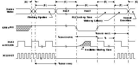
Table 5-17 HALT Mode Switching Characteristics
| PARAMETER | MIN | TYP | MAX | UNIT | |
|---|---|---|---|---|---|
| td(IDLE-XCOL) | Delay time, IDLE instruction executed to XCLKOUT low | 32tc(SCO) | 45tc(SCO) | cycles | |
| tp | PLL lock-up time | 131072tc(OSCCLK) | cycles | ||
| td(WAKE-HALT) | Delay time, PLL lock to program execution resume
|
1125tc(SCO) | cycles | ||
|
35tc(SCO) | cycles | |||

A. IDLE instruction is executed to put the device into HALT mode.
B. The PLL block responds to the HALT signal. SYSCLKOUT is held for approximately 32 cycles (if CLKINDIV = 0) or 64 cycles (if CLKINDIV = 1) before the oscillator is turned off and the CLKIN to the core is stopped. This delay enables the CPU pipe and any other pending operations to flush properly.
C. Clocks to the peripherals are turned off and the PLL is shut down. If a quartz crystal or ceramic resonator is used as the clock source, the internal oscillator is shut down as well. The device is now in HALT mode and consumes absolute minimum power.
D. When the GPIOn pin (used to bring the device out of HALT) is driven low, the oscillator is turned on and the oscillator wake-up sequence is initiated. The GPIO pin should be driven high only after the oscillator has stabilized. This enables the provision of a clean clock signal during the PLL lock sequence. Since the falling edge of the GPIO pin asynchronously begins the wakeup process, care should be taken to maintain a low noise environment prior to entering and during HALT mode.
E. Once the oscillator has stabilized, the PLL lock sequence is initiated, which takes 131,072 OSCCLK (X1/X2 or X1 or XCLKIN) cycles. Note that these 131,072 clock cycles are applicable even when the PLL is disabled (that is, code execution will be delayed by this duration even when the PLL is disabled).
F. Clocks to the core and peripherals are enabled. The HALT mode is now exited. The device will respond to the interrupt (if enabled), after a latency.
G. Normal operation resumes.
H. The wake-up signal fed to a GPIO pin to wake up the device must meet the minimum pulse width requirement. Furthermore, this signal must be free of glitches. If a noisy signal is fed to a GPIO pin, the wake-up behavior of the device will not be deterministic.
I. From the time the IDLE instruction is executed to place the device into low-power mode (LPM), wakeup should not be initiated until at least 4 OSCCLK cycles have elapsed.
Figure 5-11 HALT Wake-Up Using GPIOn