SPRS357D August 2006 – June 2020 TMS320F28044
PRODUCTION DATA.
- 1Device Overview
- 2Revision History
- 3Device Comparison
- 4Terminal Configuration and Functions
-
5Specifications
- 5.1 Absolute Maximum Ratings
- 5.2 ESD Ratings – Commercial
- 5.3 Recommended Operating Conditions
- 5.4 Power Consumption Summary
- 5.5 Electrical Characteristics
- 5.6 Thermal Resistance Characteristics for F28044 100-Ball GGM Package
- 5.7 Thermal Resistance Characteristics for F28044 100-Pin PZ Package
- 5.8 Thermal Design Considerations
- 5.9
Timing and Switching Characteristics
- 5.9.1 Timing Parameter Symbology
- 5.9.2 Power Sequencing
- 5.9.3 Clock Requirements and Characteristics
- 5.9.4
Peripherals
- 5.9.4.1 General-Purpose Input/Output (GPIO)
- 5.9.4.2 Enhanced Control Peripherals
- 5.9.4.3 External Interrupt Timing
- 5.9.4.4 I2C Electrical Specification and Timing
- 5.9.4.5 Serial Peripheral Interface (SPI) Master Mode Timing
- 5.9.4.6 SPI Slave Mode Timing
- 5.9.5 JTAG Debug Probe Connection Without Signal Buffering for the DSP
- 5.9.6 Flash Timing
- 5.10 On-Chip Analog-to-Digital Converter
-
6Detailed Description
- 6.1
Brief Descriptions
- 6.1.1 C28x CPU
- 6.1.2 Memory Bus (Harvard Bus Architecture)
- 6.1.3 Peripheral Bus
- 6.1.4 Real-Time JTAG and Analysis
- 6.1.5 Flash
- 6.1.6 M0, M1 SARAMs
- 6.1.7 L0, L1 SARAMs
- 6.1.8 Boot ROM
- 6.1.9 Security
- 6.1.10 Peripheral Interrupt Expansion (PIE) Block
- 6.1.11 External Interrupts (XINT1, XINT2, XNMI)
- 6.1.12 Oscillator and PLL
- 6.1.13 Watchdog
- 6.1.14 Peripheral Clocking
- 6.1.15 Low-Power Modes
- 6.1.16 Peripheral Frames 0, 1, 2 (PFn)
- 6.1.17 General-Purpose Input/Output (GPIO) Multiplexer
- 6.1.18 32-Bit CPU-Timers (0, 1, 2)
- 6.1.19 Control Peripherals
- 6.1.20 Serial Port Peripherals
- 6.2
Peripherals
- 6.2.1 32-Bit CPU-Timers 0/1/2
- 6.2.2 Enhanced PWM Modules (ePWM1–16)
- 6.2.3 Hi-Resolution PWM (HRPWM)
- 6.2.4 Enhanced Analog-to-Digital Converter (ADC) Module
- 6.2.5 Serial Communications Interface (SCI) Module (SCI-A)
- 6.2.6 Serial Peripheral Interface (SPI) Module (SPI-A)
- 6.2.7 Inter-Integrated Circuit (I2C)
- 6.2.8 GPIO MUX
- 6.3 Memory Map
- 6.4 Register Map
- 6.5 Interrupts
- 6.6 System Control
- 6.7 Low-Power Modes Block
- 6.1
Brief Descriptions
- 7Applications, Implementation, and Layout
- 8Device and Documentation Support
- 9Mechanical, Packaging, and Orderable Information
パッケージ・オプション
デバイスごとのパッケージ図は、PDF版データシートをご参照ください。
メカニカル・データ(パッケージ|ピン)
- PZ|100
サーマルパッド・メカニカル・データ
- PZ|100
発注情報
6.2.7 Inter-Integrated Circuit (I2C)
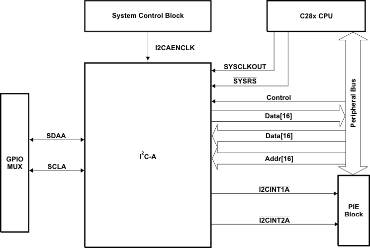
The F28044 device contains one I2C Serial Port. Figure 6-10 shows how the I2C peripheral module interfaces within the F28044 device.
The I2C module has the following features:
- Compliance with the Philips Semiconductors I2C-bus specification (version 2.1):
- Support for 1-bit to 8-bit format transfers
- 7-bit and 10-bit addressing modes
- General call
- START byte mode
- Support for multiple master-transmitters and slave-receivers
- Support for multiple slave-transmitters and master-receivers
- Combined master transmit/receive and receive/transmit mode
- Data transfer rate from 10 kbps up to 400 kbps (I2C Fast-mode rate)
- One 16-word receive FIFO and one 16-word transmit FIFO
- One interrupt that can be used by the CPU. This interrupt can be generated as a result of one of the following conditions:
- Transmit-data ready
- Receive-data ready
- Register-access ready
- No-acknowledgment received
- Arbitration lost
- Stop condition detected
- Addressed as slave
- An additional interrupt that can be used by the CPU when in FIFO mode
- Module enable/disable capability
- Free data format mode

A. The I2C registers are accessed at the SYSCLKOUT rate. The internal timing and signal waveforms of the I2C port are also at the SYSCLKOUT rate.
B. The clock enable bit (I2CAENCLK) in the PCLKCRO register turns off the clock to the I2C port for low power operation. Upon reset, I2CAENCLK is clear, which indicates the peripheral internal clocks are off.
Figure 6-10 I2C Peripheral Module Interfaces The registers in Table 6-10 configure and control the I2C port operation.
Table 6-10 I2C-A Registers
| NAME | ADDRESS | DESCRIPTION |
|---|---|---|
| I2COAR | 0x7900 | I2C own address register |
| I2CIER | 0x7901 | I2C interrupt enable register |
| I2CSTR | 0x7902 | I2C status register |
| I2CCLKL | 0x7903 | IC clock low-time divider register |
| I2CCLKH | 0x7904 | I2C clock high-time divider register |
| I2CCNT | 0x7905 | I2C data count register |
| I2CDRR | 0x7906 | I2C data receive register |
| I2CSAR | 0x7907 | I2C slave address register |
| I2CDXR | 0x7908 | I2C data transmit register |
| I2CMDR | 0x7909 | I2C mode register |
| I2CISRC | 0x790A | I2C interrupt source register |
| I2CPSC | 0x790C | I2C prescaler register |
| I2CFFTX | 0x7920 | I2C FIFO transmit register |
| I2CFFRX | 0x7921 | I2C FIFO receive register |
| I2CRSR | - | I2C receive shift register (not accessible to the CPU) |
| I2CXSR | - | I2C transmit shift register (not accessible to the CPU) |