SPRS357D August 2006 – June 2020 TMS320F28044
PRODUCTION DATA.
- 1Device Overview
- 2Revision History
- 3Device Comparison
- 4Terminal Configuration and Functions
-
5Specifications
- 5.1 Absolute Maximum Ratings
- 5.2 ESD Ratings – Commercial
- 5.3 Recommended Operating Conditions
- 5.4 Power Consumption Summary
- 5.5 Electrical Characteristics
- 5.6 Thermal Resistance Characteristics for F28044 100-Ball GGM Package
- 5.7 Thermal Resistance Characteristics for F28044 100-Pin PZ Package
- 5.8 Thermal Design Considerations
- 5.9
Timing and Switching Characteristics
- 5.9.1 Timing Parameter Symbology
- 5.9.2 Power Sequencing
- 5.9.3 Clock Requirements and Characteristics
- 5.9.4
Peripherals
- 5.9.4.1 General-Purpose Input/Output (GPIO)
- 5.9.4.2 Enhanced Control Peripherals
- 5.9.4.3 External Interrupt Timing
- 5.9.4.4 I2C Electrical Specification and Timing
- 5.9.4.5 Serial Peripheral Interface (SPI) Master Mode Timing
- 5.9.4.6 SPI Slave Mode Timing
- 5.9.5 JTAG Debug Probe Connection Without Signal Buffering for the DSP
- 5.9.6 Flash Timing
- 5.10 On-Chip Analog-to-Digital Converter
-
6Detailed Description
- 6.1
Brief Descriptions
- 6.1.1 C28x CPU
- 6.1.2 Memory Bus (Harvard Bus Architecture)
- 6.1.3 Peripheral Bus
- 6.1.4 Real-Time JTAG and Analysis
- 6.1.5 Flash
- 6.1.6 M0, M1 SARAMs
- 6.1.7 L0, L1 SARAMs
- 6.1.8 Boot ROM
- 6.1.9 Security
- 6.1.10 Peripheral Interrupt Expansion (PIE) Block
- 6.1.11 External Interrupts (XINT1, XINT2, XNMI)
- 6.1.12 Oscillator and PLL
- 6.1.13 Watchdog
- 6.1.14 Peripheral Clocking
- 6.1.15 Low-Power Modes
- 6.1.16 Peripheral Frames 0, 1, 2 (PFn)
- 6.1.17 General-Purpose Input/Output (GPIO) Multiplexer
- 6.1.18 32-Bit CPU-Timers (0, 1, 2)
- 6.1.19 Control Peripherals
- 6.1.20 Serial Port Peripherals
- 6.2
Peripherals
- 6.2.1 32-Bit CPU-Timers 0/1/2
- 6.2.2 Enhanced PWM Modules (ePWM1–16)
- 6.2.3 Hi-Resolution PWM (HRPWM)
- 6.2.4 Enhanced Analog-to-Digital Converter (ADC) Module
- 6.2.5 Serial Communications Interface (SCI) Module (SCI-A)
- 6.2.6 Serial Peripheral Interface (SPI) Module (SPI-A)
- 6.2.7 Inter-Integrated Circuit (I2C)
- 6.2.8 GPIO MUX
- 6.3 Memory Map
- 6.4 Register Map
- 6.5 Interrupts
- 6.6 System Control
- 6.7 Low-Power Modes Block
- 6.1
Brief Descriptions
- 7Applications, Implementation, and Layout
- 8Device and Documentation Support
- 9Mechanical, Packaging, and Orderable Information
パッケージ・オプション
デバイスごとのパッケージ図は、PDF版データシートをご参照ください。
メカニカル・データ(パッケージ|ピン)
- PZ|100
サーマルパッド・メカニカル・データ
- PZ|100
発注情報
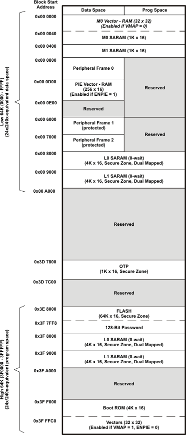
6.3 Memory Map

Table 6-13 Addresses of Flash Sectors
| ADDRESS RANGE | PROGRAM AND DATA SPACE |
|---|---|
| 0x3E 8000 – 0x3E BFFF | Sector D (16K x 16) |
| 0x3E C000 – 0x3E FFFF | Sector C (16K x 16) |
| 0x3F 0000 – 0x3F 3FFF | Sector B (16K x 16) |
| 0x3F 4000 – 0x3F 7F7F | Sector A (16K x 16) |
| 0x3F 7F80 – 0x3F 7FF5 | Program to 0x0000 when using the
Code Security Module |
| 0x3F 7FF6 – 0x3F 7FF7 | Boot-to-Flash Entry Point
(program branch instruction here) |
| 0x3F 7FF8 – 0x3F 7FFF | Security Password (128-Bit)
(Do not program to all zeros) |
NOTE
- When the code-security passwords are programmed, all addresses between 0x3F7F80 and 0x3F7FF5 cannot be used as program code or data. These locations must be programmed to 0x0000.
- If the code security feature is not used, addresses 0x3F7F80 through 0x3F7FEF may be used for code or data. Addresses 0x3F7FF0 – 0x3F7FF5 are reserved for data and should not contain program code.
Table 6-14 shows how to handle these memory locations.
Table 6-14 Impact of Using the Code Security Module
| ADDRESS | FLASH | |
|---|---|---|
| Code security enabled | Code security disabled | |
| 0x3F 7F80 – 0x3F 7FEF | Fill with 0x0000 | Application code and data |
| 0x3F 7FF0 – 0x3F 7FF5 | Reserved for data only | |
| 0x3D 7BFC – 0x3D 7BFF | Application code and data | |
Peripheral Frame 1 and Peripheral Frame 2 are grouped together so as to enable these blocks to be write/read peripheral block protected. The protected mode ensures that all accesses to these blocks happen as written. Because of the C28x pipeline, a write immediately followed by a read, to different memory locations, will appear in reverse order on the memory bus of the CPU. This can cause problems in certain peripheral applications where the user expected the write to occur first (as written). The C28x CPU supports a block protection mode where a region of memory can be protected so as to make sure that operations occur as written (the penalty is extra cycles are added to align the operations). This mode is programmable and by default, it will protect the selected zones.
The wait-states for the various spaces in the memory map area are listed in Table 6-15.
Table 6-15 Wait-states
| AREA | WAIT-STATES | COMMENTS |
|---|---|---|
| M0 and M1 SARAMs | 0-wait | Fixed |
| Peripheral Frame 0 | 0-wait | Fixed |
| Peripheral Frame 1 | 0-wait (writes)
2-wait (reads) |
Fixed. Consecutive (back-to-back) writes to Peripheral Frame 1 registers will experience a 1-cycle pipeline hit (1-cycle delay). |
| Peripheral Frame 2 | 0-wait (writes)
2-wait (reads) |
Fixed |
| L0 and L1 SARAMs | 0-wait | |
| OTP | Programmable,
1-wait minimum |
Programmed via the Flash registers. 1-wait-state operation is possible at a reduced CPU frequency. See Section 6.1.5 for more information. |
| Flash | Programmable,
0-wait minimum |
Programmed via the Flash registers. 0-wait-state operation is possible at reduced CPU frequency. The CSM password locations are hardwired for 16 wait-states. See Section 6.1.5 for more information. |
| Boot-ROM | 1-wait | Fixed |