SPRS357D August   2006  – June 2020 TMS320F28044

PRODUCTION DATA.  

  1. 1Device Overview
    1. 1.1 Features
    2. 1.2 Applications
    3. 1.3 Description
    4. 1.4 Functional Block Diagram
  2. 2Revision History
  3. 3Device Comparison
    1. 3.1 Related Products
  4. 4Terminal Configuration and Functions
    1. 4.1 Pin Diagrams
    2. 4.2 Signal Descriptions
  5. 5Specifications
    1. 5.1  Absolute Maximum Ratings
    2. 5.2  ESD Ratings – Commercial
    3. 5.3  Recommended Operating Conditions
    4. 5.4  Power Consumption Summary
      1. Table 5-1 TMS320F28044 Current Consumption by Power-Supply Pins at 100-MHz SYSCLKOUT
      2. 5.4.1     Reducing Current Consumption
    5. 5.5  Electrical Characteristics
    6. 5.6  Thermal Resistance Characteristics for F28044 100-Ball GGM Package
    7. 5.7  Thermal Resistance Characteristics for F28044 100-Pin PZ Package
    8. 5.8  Thermal Design Considerations
    9. 5.9  Timing and Switching Characteristics
      1. 5.9.1 Timing Parameter Symbology
        1. 5.9.1.1 General Notes on Timing Parameters
        2. 5.9.1.2 Test Load Circuit
        3. 5.9.1.3 Device Clock Table
          1. Table 5-3 TMS320x280x Clock Table and Nomenclature
      2. 5.9.2 Power Sequencing
        1. 5.9.2.1   Power Management and Supervisory Circuit Solutions
        2. Table 5-5 Reset (XRS) Timing Requirements
      3. 5.9.3 Clock Requirements and Characteristics
        1. Table 5-6 Input Clock Frequency
        2. Table 5-7 XCLKIN Timing Requirements - PLL Enabled
        3. Table 5-8 XCLKIN Timing Requirements - PLL Disabled
        4. Table 5-9 XCLKOUT Switching Characteristics (PLL Bypassed or Enabled)
      4. 5.9.4 Peripherals
        1. 5.9.4.1 General-Purpose Input/Output (GPIO)
          1. 5.9.4.1.1 GPIO - Output Timing
            1. Table 5-10 General-Purpose Output Switching Characteristics
          2. 5.9.4.1.2 GPIO - Input Timing
            1. Table 5-11 General-Purpose Input Timing Requirements
          3. 5.9.4.1.3 Sampling Window Width for Input Signals
          4. 5.9.4.1.4 Low-Power Mode Wakeup Timing
            1. Table 5-12 IDLE Mode Timing Requirements
            2. Table 5-13 IDLE Mode Switching Characteristics
            3. Table 5-14 STANDBY Mode Timing Requirements
            4. Table 5-15 STANDBY Mode Switching Characteristics
            5. Table 5-16 HALT Mode Timing Requirements
            6. Table 5-17 HALT Mode Switching Characteristics
        2. 5.9.4.2 Enhanced Control Peripherals
          1. 5.9.4.2.1 Enhanced Pulse Width Modulator (ePWM) Timing
            1. Table 5-18 ePWM Timing Requirements
            2. Table 5-19 ePWM Switching Characteristics
          2. 5.9.4.2.2 Trip-Zone Input Timing
            1. Table 5-20 Trip-Zone input Timing Requirements
          3. 5.9.4.2.3 High-Resolution PWM Timing
            1. Table 5-21 High Resolution PWM Characteristics at SYSCLKOUT = (60 - 100 MHz)
          4. 5.9.4.2.4 ADC Start-of-Conversion Timing
            1. Table 5-22 External ADC Start-of-Conversion Switching Characteristics
        3. 5.9.4.3 External Interrupt Timing
          1. Table 5-23 External Interrupt Timing Requirements
          2. Table 5-24 External Interrupt Switching Characteristics
        4. 5.9.4.4 I2C Electrical Specification and Timing
          1. Table 5-25 I2C Timing
        5. 5.9.4.5 Serial Peripheral Interface (SPI) Master Mode Timing
          1. Table 5-26 SPI Master Mode External Timing (Clock Phase = 0)
          2. Table 5-27 SPI Master Mode External Timing (Clock Phase = 1)
        6. 5.9.4.6 SPI Slave Mode Timing
          1. Table 5-28 SPI Slave Mode External Timing (Clock Phase = 0)
          2. Table 5-29 SPI Slave Mode External Timing (Clock Phase = 1)
      5. 5.9.5 JTAG Debug Probe Connection Without Signal Buffering for the DSP
      6. 5.9.6 Flash Timing
        1. Table 5-30 Flash Endurance for A Temperature Material
        2. Table 5-31 Flash Parameters at 100-MHz SYSCLKOUT
        3. Table 5-32 Flash/OTP Access Timing
        4. Table 5-33 Flash Data Retention Duration
    10. 5.10 On-Chip Analog-to-Digital Converter
      1. Table 5-35 ADC Electrical Characteristics (over recommended operating conditions)
      2. 5.10.1     ADC Power-Up Control Bit Timing
        1. Table 5-36 ADC Power-Up Delays
        2. Table 5-37 Current Consumption for Different ADC Configurations (at 25-MHz ADCCLK)
      3. 5.10.2     Definitions
      4. 5.10.3     Sequential Sampling Mode (Single-Channel) (SMODE = 0)
        1. Table 5-38 Sequential Sampling Mode Timing
      5. 5.10.4     Simultaneous Sampling Mode (Dual-Channel) (SMODE = 1)
        1. Table 5-39 Simultaneous Sampling Mode Timing
      6. 5.10.5     Detailed Descriptions
  6. 6Detailed Description
    1. 6.1 Brief Descriptions
      1. 6.1.1  C28x CPU
      2. 6.1.2  Memory Bus (Harvard Bus Architecture)
      3. 6.1.3  Peripheral Bus
      4. 6.1.4  Real-Time JTAG and Analysis
      5. 6.1.5  Flash
      6. 6.1.6  M0, M1 SARAMs
      7. 6.1.7  L0, L1 SARAMs
      8. 6.1.8  Boot ROM
      9. 6.1.9  Security
      10. 6.1.10 Peripheral Interrupt Expansion (PIE) Block
      11. 6.1.11 External Interrupts (XINT1, XINT2, XNMI)
      12. 6.1.12 Oscillator and PLL
      13. 6.1.13 Watchdog
      14. 6.1.14 Peripheral Clocking
      15. 6.1.15 Low-Power Modes
      16. 6.1.16 Peripheral Frames 0, 1, 2 (PFn)
      17. 6.1.17 General-Purpose Input/Output (GPIO) Multiplexer
      18. 6.1.18 32-Bit CPU-Timers (0, 1, 2)
      19. 6.1.19 Control Peripherals
      20. 6.1.20 Serial Port Peripherals
    2. 6.2 Peripherals
      1. 6.2.1 32-Bit CPU-Timers 0/1/2
      2. 6.2.2 Enhanced PWM Modules (ePWM1–16)
      3. 6.2.3 Hi-Resolution PWM (HRPWM)
      4. 6.2.4 Enhanced Analog-to-Digital Converter (ADC) Module
        1. 6.2.4.1 ADC Connections if the ADC Is Not Used
        2. 6.2.4.2 ADC Registers
      5. 6.2.5 Serial Communications Interface (SCI) Module (SCI-A)
      6. 6.2.6 Serial Peripheral Interface (SPI) Module (SPI-A)
      7. 6.2.7 Inter-Integrated Circuit (I2C)
      8. 6.2.8 GPIO MUX
    3. 6.3 Memory Map
    4. 6.4 Register Map
      1. 6.4.1 Device Emulation Registers
    5. 6.5 Interrupts
      1. 6.5.1 External Interrupts
    6. 6.6 System Control
      1. 6.6.1 OSC and PLL Block
        1. 6.6.1.1 External Reference Oscillator Clock Option
        2. 6.6.1.2 PLL-Based Clock Module
        3. 6.6.1.3 Loss of Input Clock
      2. 6.6.2 Watchdog Block
    7. 6.7 Low-Power Modes Block
  7. 7Applications, Implementation, and Layout
    1. 7.1 TI Reference Design
  8. 8Device and Documentation Support
    1. 8.1 Getting Started
    2. 8.2 Device and Development Support Tool Nomenclature
    3. 8.3 Tools and Software
    4. 8.4 Documentation Support
    5. 8.5 Support Resources
    6. 8.6 Trademarks
    7. 8.7 Electrostatic Discharge Caution
    8. 8.8 Glossary
  9. 9Mechanical, Packaging, and Orderable Information
    1. 9.1 Packaging Information

パッケージ・オプション

デバイスごとのパッケージ図は、PDF版データシートをご参照ください。

メカニカル・データ(パッケージ|ピン)
  • PZ|100
サーマルパッド・メカニカル・データ
発注情報

Watchdog Block

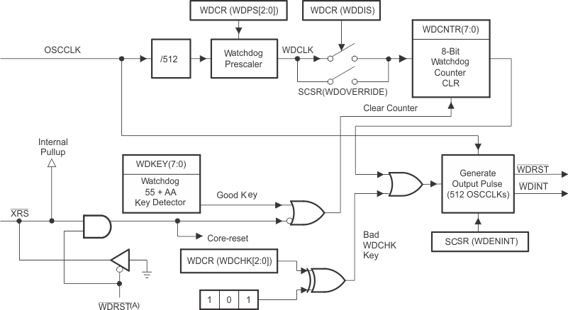
The watchdog block on the F28044 is similar to the one used on the 240x and 281x devices. The watchdog module generates an output pulse, 512 oscillator clocks wide (OSCCLK), whenever the 8-bit watchdog up counter has reached its maximum value. To prevent this, the user disables the counter or the software must periodically write a 0x55 + 0xAA sequence into the watchdog key register which will reset the watchdog counter. Figure 6-21 shows the various functional blocks within the watchdog module.

TMS320F28044 wdmod_prs357.gif
The WDRST signal is driven low for 512 OSCCLK cycles.
Figure 6-21 Watchdog Module

The WDINT signal enables the watchdog to be used as a wakeup from IDLE/STANDBY mode.

In STANDBY mode, all peripherals are turned off on the device. The only peripheral that remains functional is the watchdog. The WATCHDOG module will run off OSCCLK. The WDINT signal is fed to the LPM block so that it can wake the device from STANDBY (if enabled). See Section 6.7, Low-Power Modes Block, for details.

In IDLE mode, the WDINT signal can generate an interrupt to the CPU, via the PIE, to take the CPU out of IDLE mode.

In HALT mode, this feature cannot be used because the oscillator (and PLL) are turned off and hence so is the WATCHDOG.