JAJS280O October 2003 – March 2019 TMS320F2801 , TMS320F28015 , TMS320F28016 , TMS320F2802 , TMS320F2806 , TMS320F2808 , TMS320F2809
PRODUCTION DATA.
- 1デバイスの概要
- 2改訂履歴
- 3Device Comparison
- 4Terminal Configuration and Functions
-
5Specifications
- 5.1 Absolute Maximum Ratings
- 5.2 ESD Ratings – Automotive
- 5.3 ESD Ratings – Commercial
- 5.4 Recommended Operating Conditions
- 5.5
Power Consumption Summary
- Table 5-1 TMS320F2809, TMS320F2808 Current Consumption by Power-Supply Pins at 100-MHz SYSCLKOUT
- Table 5-2 TMS320F2806 Current Consumption by Power-Supply Pins at 100-MHz SYSCLKOUT
- Table 5-3 TMS320F2802, TMS320F2801 Current Consumption by Power-Supply Pins at 100-MHz SYSCLKOUT
- Table 5-4 TMS320C2802, TMS320C2801 Current Consumption by Power-Supply Pins at 100-MHz SYSCLKOUT
- 5.5.1 Reducing Current Consumption
- 5.5.2 Current Consumption Graphs
- 5.6 Electrical Characteristics
- 5.7 Thermal Resistance Characteristics for F280x 100-Ball GGM Package
- 5.8 Thermal Resistance Characteristics for F280x 100-Pin PZ Package
- 5.9 Thermal Resistance Characteristics for C280x 100-Ball GGM Package
- 5.10 Thermal Resistance Characteristics for C280x 100-Pin PZ Package
- 5.11 Thermal Resistance Characteristics for F2809 100-Ball GGM Package
- 5.12 Thermal Resistance Characteristics for F2809 100-Pin PZ Package
- 5.13 Thermal Design Considerations
- 5.14
Timing and Switching Characteristics
- 5.14.1 Timing Parameter Symbology
- 5.14.2 Power Sequencing
- 5.14.3 Clock Requirements and Characteristics
- 5.14.4
Peripherals
- 5.14.4.1 General-Purpose Input/Output (GPIO)
- 5.14.4.2 Enhanced Control Peripherals
- 5.14.4.3 External Interrupt Timing
- 5.14.4.4 I2C Electrical Specification and Timing
- 5.14.4.5 Serial Peripheral Interface (SPI) Timing
- 5.14.5 Emulator Connection Without Signal Buffering for the DSP
- 5.14.6 Flash Timing
- 5.15 On-Chip Analog-to-Digital Converter
- 5.16 Migrating From F280x Devices to C280x Devices
- 5.17 ROM Timing (C280x only)
-
6Detailed Description
- 6.1
Brief Descriptions
- 6.1.1 C28x CPU
- 6.1.2 Memory Bus (Harvard Bus Architecture)
- 6.1.3 Peripheral Bus
- 6.1.4 Real-Time JTAG and Analysis
- 6.1.5 Flash
- 6.1.6 ROM
- 6.1.7 M0, M1 SARAMs
- 6.1.8 L0, L1, H0 SARAMs
- 6.1.9 Boot ROM
- 6.1.10 Security
- 6.1.11 Peripheral Interrupt Expansion (PIE) Block
- 6.1.12 External Interrupts (XINT1, XINT2, XNMI)
- 6.1.13 Oscillator and PLL
- 6.1.14 Watchdog
- 6.1.15 Peripheral Clocking
- 6.1.16 Low-Power Modes
- 6.1.17 Peripheral Frames 0, 1, 2 (PFn)
- 6.1.18 General-Purpose Input/Output (GPIO) Multiplexer
- 6.1.19 32-Bit CPU-Timers (0, 1, 2)
- 6.1.20 Control Peripherals
- 6.1.21 Serial Port Peripherals
- 6.2
Peripherals
- 6.2.1 32-Bit CPU-Timers 0/1/2
- 6.2.2 Enhanced PWM Modules (ePWM1/2/3/4/5/6)
- 6.2.3 Hi-Resolution PWM (HRPWM)
- 6.2.4 Enhanced CAP Modules (eCAP1/2/3/4)
- 6.2.5 Enhanced QEP Modules (eQEP1/2)
- 6.2.6 Enhanced Analog-to-Digital Converter (ADC) Module
- 6.2.7 Enhanced Controller Area Network (eCAN) Modules (eCAN-A and eCAN-B)
- 6.2.8 Serial Communications Interface (SCI) Modules (SCI-A, SCI-B)
- 6.2.9 Serial Peripheral Interface (SPI) Modules (SPI-A, SPI-B, SPI-C, SPI-D)
- 6.2.10 Inter-Integrated Circuit (I2C)
- 6.2.11 GPIO MUX
- 6.3 Memory Maps
- 6.4 Register Map
- 6.5 Interrupts
- 6.6 System Control
- 6.7 Low-Power Modes Block
- 6.1
Brief Descriptions
- 7Applications, Implementation, and Layout
- 8デバイスおよびドキュメントのサポート
- 9メカニカル、パッケージ、および注文情報
パッケージ・オプション
デバイスごとのパッケージ図は、PDF版データシートをご参照ください。
メカニカル・データ(パッケージ|ピン)
- PZ|100
- NMF|100
サーマルパッド・メカニカル・データ
- PZ|100
発注情報
6.2.4 Enhanced CAP Modules (eCAP1/2/3/4)
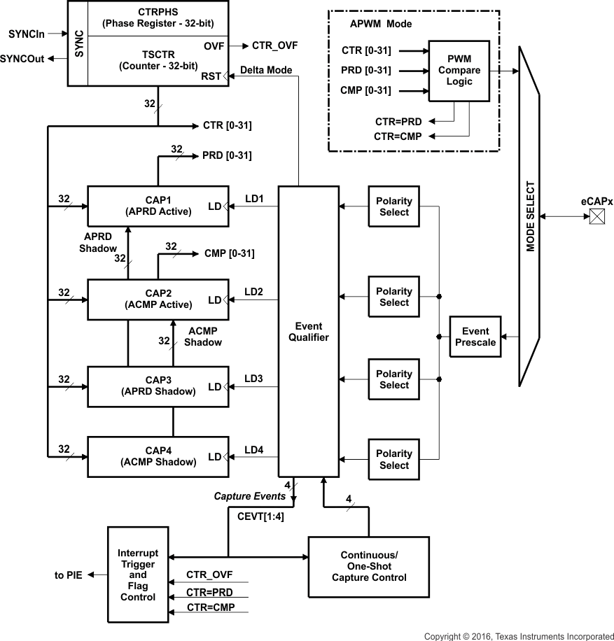
The 280x device contains up to four enhanced capture (eCAP) modules. Figure 6-5 shows a functional block diagram of a module. See the TMS320x280x, 2801x, 2804x Enhanced Capture (eCAP) module reference guide for more details.
 Figure 6-5 eCAP Functional Block Diagram
 The eCAP modules are clocked at the SYSCLKOUT rate.
The clock enable bits (ECAP1/2/3/4ENCLK) in the PCLKCR1 register are used to turn off the eCAP modules individually (for low power operation). Upon reset, ECAP1ENCLK, ECAP2ENCLK, ECAP3ENCLK, and ECAP4ENCLK are set to low, indicating that the peripheral clock is off.
Table 6-4 eCAP Control and Status Registers
| NAME | eCAP1 | eCAP2 | eCAP3 | eCAP4 | SIZE (x16) | DESCRIPTION |
|---|---|---|---|---|---|---|
| TSCTR | 0x6A00 | 0x6A20 | 0x6A40 | 0x6A60 | 2 | Time-Stamp Counter |
| CTRPHS | 0x6A02 | 0x6A22 | 0x6A42 | 0x6A62 | 2 | Counter Phase Offset Value Register |
| CAP1 | 0x6A04 | 0x6A24 | 0x6A44 | 0x6A64 | 2 | Capture 1 Register |
| CAP2 | 0x6A06 | 0x6A26 | 0x6A46 | 0x6A66 | 2 | Capture 2 Register |
| CAP3 | 0x6A08 | 0x6A28 | 0x6A48 | 0x6A68 | 2 | Capture 3 Register |
| CAP4 | 0x6A0A | 0x6A2A | 0x6A4A | 0x6A6A | 2 | Capture 4 Register |
| Reserved | 0x6A0C – 0x6A12 | 0x6A2C – 0x6A32 | 0x6A4C – 0x6A52 | 0x6A6C – 0x6A72 | 8 | Reserved |
| ECCTL1 | 0x6A14 | 0x6A34 | 0x6A54 | 0x6A74 | 1 | Capture Control Register 1 |
| ECCTL2 | 0x6A15 | 0x6A35 | 0x6A55 | 0x6A75 | 1 | Capture Control Register 2 |
| ECEINT | 0x6A16 | 0x6A36 | 0x6A56 | 0x6A76 | 1 | Capture Interrupt Enable Register |
| ECFLG | 0x6A17 | 0x6A37 | 0x6A57 | 0x6A77 | 1 | Capture Interrupt Flag Register |
| ECCLR | 0x6A18 | 0x6A38 | 0x6A58 | 0x6A78 | 1 | Capture Interrupt Clear Register |
| ECFRC | 0x6A19 | 0x6A39 | 0x6A59 | 0x6A79 | 1 | Capture Interrupt Force Register |
| Reserved | 0x6A1A – 0x6A1F | 0x6A3A – 0x6A3F | 0x6A5A – 0x6A5F | 0x6A7A – 0x6A7F | 6 | Reserved |