JAJS280O October 2003 – March 2019 TMS320F2801 , TMS320F28015 , TMS320F28016 , TMS320F2802 , TMS320F2806 , TMS320F2808 , TMS320F2809
PRODUCTION DATA.
- 1デバイスの概要
- 2改訂履歴
- 3Device Comparison
- 4Terminal Configuration and Functions
-
5Specifications
- 5.1 Absolute Maximum Ratings
- 5.2 ESD Ratings – Automotive
- 5.3 ESD Ratings – Commercial
- 5.4 Recommended Operating Conditions
- 5.5
Power Consumption Summary
- Table 5-1 TMS320F2809, TMS320F2808 Current Consumption by Power-Supply Pins at 100-MHz SYSCLKOUT
- Table 5-2 TMS320F2806 Current Consumption by Power-Supply Pins at 100-MHz SYSCLKOUT
- Table 5-3 TMS320F2802, TMS320F2801 Current Consumption by Power-Supply Pins at 100-MHz SYSCLKOUT
- Table 5-4 TMS320C2802, TMS320C2801 Current Consumption by Power-Supply Pins at 100-MHz SYSCLKOUT
- 5.5.1 Reducing Current Consumption
- 5.5.2 Current Consumption Graphs
- 5.6 Electrical Characteristics
- 5.7 Thermal Resistance Characteristics for F280x 100-Ball GGM Package
- 5.8 Thermal Resistance Characteristics for F280x 100-Pin PZ Package
- 5.9 Thermal Resistance Characteristics for C280x 100-Ball GGM Package
- 5.10 Thermal Resistance Characteristics for C280x 100-Pin PZ Package
- 5.11 Thermal Resistance Characteristics for F2809 100-Ball GGM Package
- 5.12 Thermal Resistance Characteristics for F2809 100-Pin PZ Package
- 5.13 Thermal Design Considerations
- 5.14
Timing and Switching Characteristics
- 5.14.1 Timing Parameter Symbology
- 5.14.2 Power Sequencing
- 5.14.3 Clock Requirements and Characteristics
- 5.14.4
Peripherals
- 5.14.4.1 General-Purpose Input/Output (GPIO)
- 5.14.4.2 Enhanced Control Peripherals
- 5.14.4.3 External Interrupt Timing
- 5.14.4.4 I2C Electrical Specification and Timing
- 5.14.4.5 Serial Peripheral Interface (SPI) Timing
- 5.14.5 Emulator Connection Without Signal Buffering for the DSP
- 5.14.6 Flash Timing
- 5.15 On-Chip Analog-to-Digital Converter
- 5.16 Migrating From F280x Devices to C280x Devices
- 5.17 ROM Timing (C280x only)
-
6Detailed Description
- 6.1
Brief Descriptions
- 6.1.1 C28x CPU
- 6.1.2 Memory Bus (Harvard Bus Architecture)
- 6.1.3 Peripheral Bus
- 6.1.4 Real-Time JTAG and Analysis
- 6.1.5 Flash
- 6.1.6 ROM
- 6.1.7 M0, M1 SARAMs
- 6.1.8 L0, L1, H0 SARAMs
- 6.1.9 Boot ROM
- 6.1.10 Security
- 6.1.11 Peripheral Interrupt Expansion (PIE) Block
- 6.1.12 External Interrupts (XINT1, XINT2, XNMI)
- 6.1.13 Oscillator and PLL
- 6.1.14 Watchdog
- 6.1.15 Peripheral Clocking
- 6.1.16 Low-Power Modes
- 6.1.17 Peripheral Frames 0, 1, 2 (PFn)
- 6.1.18 General-Purpose Input/Output (GPIO) Multiplexer
- 6.1.19 32-Bit CPU-Timers (0, 1, 2)
- 6.1.20 Control Peripherals
- 6.1.21 Serial Port Peripherals
- 6.2
Peripherals
- 6.2.1 32-Bit CPU-Timers 0/1/2
- 6.2.2 Enhanced PWM Modules (ePWM1/2/3/4/5/6)
- 6.2.3 Hi-Resolution PWM (HRPWM)
- 6.2.4 Enhanced CAP Modules (eCAP1/2/3/4)
- 6.2.5 Enhanced QEP Modules (eQEP1/2)
- 6.2.6 Enhanced Analog-to-Digital Converter (ADC) Module
- 6.2.7 Enhanced Controller Area Network (eCAN) Modules (eCAN-A and eCAN-B)
- 6.2.8 Serial Communications Interface (SCI) Modules (SCI-A, SCI-B)
- 6.2.9 Serial Peripheral Interface (SPI) Modules (SPI-A, SPI-B, SPI-C, SPI-D)
- 6.2.10 Inter-Integrated Circuit (I2C)
- 6.2.11 GPIO MUX
- 6.3 Memory Maps
- 6.4 Register Map
- 6.5 Interrupts
- 6.6 System Control
- 6.7 Low-Power Modes Block
- 6.1
Brief Descriptions
- 7Applications, Implementation, and Layout
- 8デバイスおよびドキュメントのサポート
- 9メカニカル、パッケージ、および注文情報
パッケージ・オプション
デバイスごとのパッケージ図は、PDF版データシートをご参照ください。
メカニカル・データ(パッケージ|ピン)
- PZ|100
サーマルパッド・メカニカル・データ
- PZ|100
発注情報
6.2.1 32-Bit CPU-Timers 0/1/2
There are three 32-bit CPU-timers on the 280x devices (CPU-TIMER0/1/2).
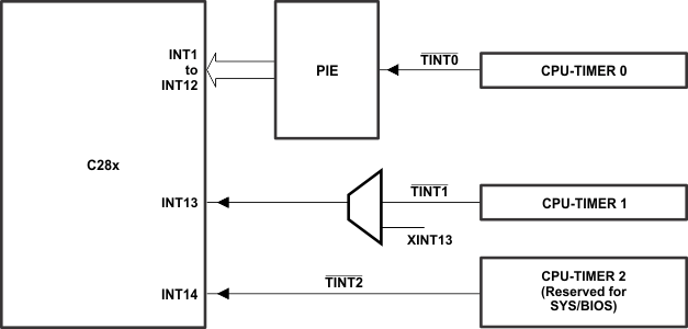
CPU-Timer 0 and CPU-Timer 1 can be used in user applications. Timer 2 is reserved for SYS/BIOS. These timers are different from the timers that are present in the ePWM modules.
NOTE
If the application is not using SYS/BIOS, then CPU-Timer 2 can be used in the application.
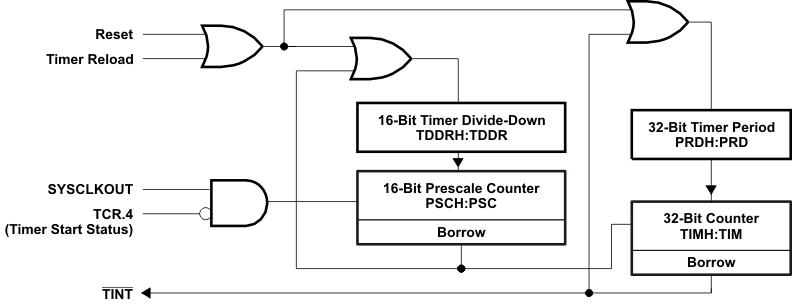
 Figure 6-1 CPU-Timers
 In the 280x devices, the timer interrupt signals (TINT0, TINT1, TINT2) are connected as shown in Figure 6-2.

The general operation of the timer is as follows: The 32-bit counter register "TIMH:TIM" is loaded with the value in the period register "PRDH:PRD". The counter register decrements at the SYSCLKOUT rate of the C28x. When the counter reaches 0, a timer interrupt output signal generates an interrupt pulse. The registers listed in Table 6-2 are used to configure the timers. For more information, see the TMS320x280x, 2801x, 2804x DSP system control and interrupts reference guide.
Table 6-2 CPU-Timers 0, 1, 2 Configuration and Control Registers
| NAME | ADDRESS | SIZE (x16) | DESCRIPTION |
|---|---|---|---|
| TIMER0TIM | 0x0C00 | 1 | CPU-Timer 0, Counter Register |
| TIMER0TIMH | 0x0C01 | 1 | CPU-Timer 0, Counter Register High |
| TIMER0PRD | 0x0C02 | 1 | CPU-Timer 0, Period Register |
| TIMER0PRDH | 0x0C03 | 1 | CPU-Timer 0, Period Register High |
| TIMER0TCR | 0x0C04 | 1 | CPU-Timer 0, Control Register |
| Reserved | 0x0C05 | 1 | Reserved |
| TIMER0TPR | 0x0C06 | 1 | CPU-Timer 0, Prescale Register |
| TIMER0TPRH | 0x0C07 | 1 | CPU-Timer 0, Prescale Register High |
| TIMER1TIM | 0x0C08 | 1 | CPU-Timer 1, Counter Register |
| TIMER1TIMH | 0x0C09 | 1 | CPU-Timer 1, Counter Register High |
| TIMER1PRD | 0x0C0A | 1 | CPU-Timer 1, Period Register |
| TIMER1PRDH | 0x0C0B | 1 | CPU-Timer 1, Period Register High |
| TIMER1TCR | 0x0C0C | 1 | CPU-Timer 1, Control Register |
| Reserved | 0x0C0D | 1 | Reserved |
| TIMER1TPR | 0x0C0E | 1 | CPU-Timer 1, Prescale Register |
| TIMER1TPRH | 0x0C0F | 1 | CPU-Timer 1, Prescale Register High |
| TIMER2TIM | 0x0C10 | 1 | CPU-Timer 2, Counter Register |
| TIMER2TIMH | 0x0C11 | 1 | CPU-Timer 2, Counter Register High |
| TIMER2PRD | 0x0C12 | 1 | CPU-Timer 2, Period Register |
| TIMER2PRDH | 0x0C13 | 1 | CPU-Timer 2, Period Register High |
| TIMER2TCR | 0x0C14 | 1 | CPU-Timer 2, Control Register |
| Reserved | 0x0C15 | 1 | Reserved |
| TIMER2TPR | 0x0C16 | 1 | CPU-Timer 2, Prescale Register |
| TIMER2TPRH | 0x0C17 | 1 | CPU-Timer 2, Prescale Register High |
| Reserved | 0x0C18 –
0x0C3F |
40 | Reserved |