JAJSHM4U April 2001 – July 2019 TMS320F2810 , TMS320F2811 , TMS320F2812
PRODUCTION DATA.
- 1デバイスの概要
- 2改訂履歴
- 3Device Comparison
- 4Terminal Configuration and Functions
-
5Specifications
- 5.1 Absolute Maximum Ratings
- 5.2 ESD Ratings – Commercial
- 5.3 ESD Ratings – Automotive
- 5.4 Recommended Operating Conditions
- 5.5 Power Consumption Summary
- 5.6 Electrical Characteristics
- 5.7 Thermal Resistance Characteristics for 179-Ball ZHH Package
- 5.8 Thermal Resistance Characteristics for 179-Ball GHH Package
- 5.9 Thermal Resistance Characteristics for 176-Pin PGF Package
- 5.10 Thermal Resistance Characteristics for 128-Pin PBK Package
- 5.11 Thermal Design Considerations
- 5.12
Timing and Switching Characteristics
- 5.12.1 Timing Parameter Symbology
- 5.12.2 Power Supply Sequencing
- 5.12.3 Reset Timing
- 5.12.4 Clock Specifications
- 5.12.5
Peripherals
- 5.12.5.1 General-Purpose Input/Output (GPIO) – Output Timing
- 5.12.5.2 General-Purpose Input/Output (GPIO) – Input Timing
- 5.12.5.3 Event Manager Interface
- 5.12.5.4 Low-Power Mode Wakeup Timing
- 5.12.5.5 Serial Peripheral Interface (SPI) Master Mode Timing
- 5.12.5.6 Serial Peripheral Interface (SPI) Slave Mode Timing
- 5.12.5.7 External Interface (XINTF) Timing
- 5.12.5.8 XINTF Signal Alignment to XCLKOUT
- 5.12.5.9 External Interface Read Timing
- 5.12.5.10 External Interface Write Timing
- 5.12.5.11
External Interface Ready-on-Read Timing With One External Wait State
- Table 5-31 External Memory Interface Read Switching Characteristics (Ready-on-Read, 1 Wait State)
- Table 5-32 External Memory Interface Read Timing Requirements (Ready-on-Read, 1 Wait State)
- Table 5-33 Synchronous XREADY Timing Requirements (Ready-on-Read, 1 Wait State)
- Table 5-34 Asynchronous XREADY Timing Requirements (Ready-on-Read, 1 Wait State)
- 5.12.5.12 External Interface Ready-on-Write Timing With One External Wait State
- 5.12.5.13 XHOLD and XHOLDA
- 5.12.5.14 XHOLD/XHOLDA Timing
- 5.12.5.15
On-Chip Analog-to-Digital Converter
- Table 5-40 ADC Absolute Maximum Ratings Over Recommended Operating Conditions (Unless Otherwise Noted)
- Table 5-41 ADC Electrical Characteristics Over Recommended Operating Conditions (Unless Otherwise Noted)—AC Specifications
- Table 5-42 ADC Electrical Characteristics Over Recommended Operating Conditions (Unless Otherwise Noted)—DC Specifications
- 5.12.5.15.1 Current Consumption for Different ADC Configurations
- 5.12.5.15.2 ADC Power-Up Control Bit Timing
- 5.12.5.15.3 Detailed Description
- 5.12.5.15.4 Sequential Sampling Mode (Single-Channel) (SMODE = 0)
- 5.12.5.15.5 Simultaneous Sampling Mode (Dual-Channel) (SMODE = 1)
- 5.12.5.15.6 Definitions of Specifications and Terminology
- 5.12.5.16
Multichannel Buffered Serial Port (McBSP) Timing
- 5.12.5.16.1 McBSP Transmit and Receive Timing
- 5.12.5.16.2
McBSP as SPI Master or Slave Timing
- Table 5-49 McBSP as SPI Master or Slave Timing Requirements (CLKSTP = 10b, CLKXP = 0)
- Table 5-50 McBSP as SPI Master or Slave Switching Characteristics (CLKSTP = 10b, CLKXP = 0)
- Table 5-51 McBSP as SPI Master or Slave Timing Requirements (CLKSTP = 11b, CLKXP = 0)
- Table 5-52 McBSP as SPI Master or Slave Switching Characteristics (CLKSTP = 11b, CLKXP = 0)
- Table 5-53 McBSP as SPI Master or Slave Timing Requirements (CLKSTP = 10b, CLKXP = 1)
- Table 5-54 McBSP as SPI Master or Slave Switching Characteristics (CLKSTP = 10b, CLKXP = 1)
- Table 5-55 McBSP as SPI Master or Slave Timing Requirements (CLKSTP = 11b, CLKXP = 1)
- Table 5-56 McBSP as SPI Master or Slave Switching Characteristics (CLKSTP = 11b, CLKXP = 1)
- 5.12.6 Emulator Connection Without Signal Buffering for the DSP
- 5.12.7 Interrupt Timing
- 5.12.8 Flash Timing
-
6Detailed Description
- 6.1
Brief Descriptions
- 6.1.1 C28x CPU
- 6.1.2 Memory Bus (Harvard Bus Architecture)
- 6.1.3 Peripheral Bus
- 6.1.4 Real-Time JTAG and Analysis
- 6.1.5 External Interface (XINTF) (F2812 Only)
- 6.1.6 Flash
- 6.1.7 M0, M1 SARAMs
- 6.1.8 L0, L1, H0 SARAMs
- 6.1.9 Boot ROM
- 6.1.10 Security
- 6.1.11 Peripheral Interrupt Expansion (PIE) Block
- 6.1.12 External Interrupts (XINT1, XINT2, XINT13, XNMI)
- 6.1.13 Oscillator and PLL
- 6.1.14 Watchdog
- 6.1.15 Peripheral Clocking
- 6.1.16 Low-Power Modes
- 6.1.17 Peripheral Frames 0, 1, 2 (PFn)
- 6.1.18 General-Purpose Input/Output (GPIO) Multiplexer
- 6.1.19 32-Bit CPU-Timers (0, 1, 2)
- 6.1.20 Control Peripherals
- 6.1.21 Serial Port Peripherals
- 6.2
Peripherals
- 6.2.1 32-Bit CPU-Timers 0/1/2
- 6.2.2
Event Manager Modules (EVA, EVB)
- 6.2.2.1 General-Purpose (GP) Timers
- 6.2.2.2 Full-Compare Units
- 6.2.2.3 Programmable Deadband Generator
- 6.2.2.4 PWM Waveform Generation
- 6.2.2.5 Double Update PWM Mode
- 6.2.2.6 PWM Characteristics
- 6.2.2.7 Capture Unit
- 6.2.2.8 Quadrature-Encoder Pulse (QEP) Circuit
- 6.2.2.9 External ADC Start-of-Conversion
- 6.2.3 Enhanced Analog-to-Digital Converter (ADC) Module
- 6.2.4 Enhanced Controller Area Network (eCAN) Module
- 6.2.5 Multichannel Buffered Serial Port (McBSP) Module
- 6.2.6 Serial Communications Interface (SCI) Module
- 6.2.7 Serial Peripheral Interface (SPI) Module
- 6.2.8 GPIO MUX
- 6.3 Memory Maps
- 6.4 Register Map
- 6.5 Device Emulation Registers
- 6.6 External Interface, XINTF (F2812 Only)
- 6.7 Interrupts
- 6.8 System Control
- 6.9 OSC and PLL Block
- 6.10 PLL-Based Clock Module
- 6.11 External Reference Oscillator Clock Option
- 6.12 Watchdog Block
- 6.13 Low-Power Modes Block
- 6.1
Brief Descriptions
- 7Applications, Implementation, and Layout
- 8デバイスおよびドキュメントのサポート
- 9メカニカル、パッケージ、および注文情報
パッケージ・オプション
デバイスごとのパッケージ図は、PDF版データシートをご参照ください。
メカニカル・データ(パッケージ|ピン)
- PBK|128
サーマルパッド・メカニカル・データ
- PBK|128
発注情報
6.2.1 32-Bit CPU-Timers 0/1/2
There are three 32-bit CPU-timers on the F281x devices (CPU-TIMER0/1/2).
Timer 2 is reserved for DSP/BIOS. CPU-Timer 0 and CPU-Timer 1 can be used in user applications. These timers are different from the general-purpose (GP) timers that are present in the Event Manager modules (EVA, EVB).
NOTE
If the application is not using DSP/BIOS, then CPU-Timer 2 can be used in the application.
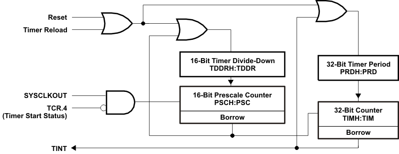
 Figure 6-1 CPU-Timers
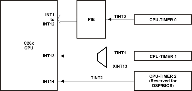
 In the F281x devices, the timer interrupt signals (TINT0, TINT1, TINT2) are connected as shown in Figure 6-2.

The general operation of the timer is as follows: The 32-bit counter register “TIMH:TIM” is loaded with the value in the period register “PRDH:PRD”. The counter register decrements at the SYSCLKOUT rate of the C28x. When the counter reaches 0, a timer interrupt output signal generates an interrupt pulse. The registers listed in Table 6-3 are used to configure the timers. For more information, see the TMS320x281x DSP System Control and Interrupts Reference Guide.
Table 6-3 CPU-Timers 0, 1, 2 Configuration and Control Registers
| NAME | ADDRESS | SIZE (x16) | DESCRIPTION |
|---|---|---|---|
| TIMER0TIM | 0x00 0C00 | 1 | CPU-Timer 0, Counter Register |
| TIMER0TIMH | 0x00 0C01 | 1 | CPU-Timer 0, Counter Register High |
| TIMER0PRD | 0x00 0C02 | 1 | CPU-Timer 0, Period Register |
| TIMER0PRDH | 0x00 0C03 | 1 | CPU-Timer 0, Period Register High |
| TIMER0TCR | 0x00 0C04 | 1 | CPU-Timer 0, Control Register |
| Reserved | 0x00 0C05 | 1 | |
| TIMER0TPR | 0x00 0C06 | 1 | CPU-Timer 0, Prescale Register |
| TIMER0TPRH | 0x00 0C07 | 1 | CPU-Timer 0, Prescale Register High |
| TIMER1TIM | 0x00 0C08 | 1 | CPU-Timer 1, Counter Register |
| TIMER1TIMH | 0x00 0C09 | 1 | CPU-Timer 1, Counter Register High |
| TIMER1PRD | 0x00 0C0A | 1 | CPU-Timer 1, Period Register |
| TIMER1PRDH | 0x00 0C0B | 1 | CPU-Timer 1, Period Register High |
| TIMER1TCR | 0x00 0C0C | 1 | CPU-Timer 1, Control Register |
| Reserved | 0x00 0C0D | 1 | |
| TIMER1TPR | 0x00 0C0E | 1 | CPU-Timer 1, Prescale Register |
| TIMER1TPRH | 0x00 0C0F | 1 | CPU-Timer 1, Prescale Register High |
| TIMER2TIM | 0x00 0C10 | 1 | CPU-Timer 2, Counter Register |
| TIMER2TIMH | 0x00 0C11 | 1 | CPU-Timer 2, Counter Register High |
| TIMER2PRD | 0x00 0C12 | 1 | CPU-Timer 2, Period Register |
| TIMER2PRDH | 0x00 0C13 | 1 | CPU-Timer 2, Period Register High |
| TIMER2TCR | 0x00 0C14 | 1 | CPU-Timer 2, Control Register |
| Reserved | 0x00 0C15 | 1 | |
| TIMER2TPR | 0x00 0C16 | 1 | CPU-Timer 2, Prescale Register |
| TIMER2TPRH | 0x00 0C17 | 1 | CPU-Timer 2, Prescale Register High |
| Reserved | 0x00 0C18 – 0x00 0C3F | 40 |