JAJSHM4U April 2001 – July 2019 TMS320F2810 , TMS320F2811 , TMS320F2812
PRODUCTION DATA.
- 1デバイスの概要
- 2改訂履歴
- 3Device Comparison
- 4Terminal Configuration and Functions
-
5Specifications
- 5.1 Absolute Maximum Ratings
- 5.2 ESD Ratings – Commercial
- 5.3 ESD Ratings – Automotive
- 5.4 Recommended Operating Conditions
- 5.5 Power Consumption Summary
- 5.6 Electrical Characteristics
- 5.7 Thermal Resistance Characteristics for 179-Ball ZHH Package
- 5.8 Thermal Resistance Characteristics for 179-Ball GHH Package
- 5.9 Thermal Resistance Characteristics for 176-Pin PGF Package
- 5.10 Thermal Resistance Characteristics for 128-Pin PBK Package
- 5.11 Thermal Design Considerations
- 5.12
Timing and Switching Characteristics
- 5.12.1 Timing Parameter Symbology
- 5.12.2 Power Supply Sequencing
- 5.12.3 Reset Timing
- 5.12.4 Clock Specifications
- 5.12.5
Peripherals
- 5.12.5.1 General-Purpose Input/Output (GPIO) – Output Timing
- 5.12.5.2 General-Purpose Input/Output (GPIO) – Input Timing
- 5.12.5.3 Event Manager Interface
- 5.12.5.4 Low-Power Mode Wakeup Timing
- 5.12.5.5 Serial Peripheral Interface (SPI) Master Mode Timing
- 5.12.5.6 Serial Peripheral Interface (SPI) Slave Mode Timing
- 5.12.5.7 External Interface (XINTF) Timing
- 5.12.5.8 XINTF Signal Alignment to XCLKOUT
- 5.12.5.9 External Interface Read Timing
- 5.12.5.10 External Interface Write Timing
- 5.12.5.11
External Interface Ready-on-Read Timing With One External Wait State
- Table 5-31 External Memory Interface Read Switching Characteristics (Ready-on-Read, 1 Wait State)
- Table 5-32 External Memory Interface Read Timing Requirements (Ready-on-Read, 1 Wait State)
- Table 5-33 Synchronous XREADY Timing Requirements (Ready-on-Read, 1 Wait State)
- Table 5-34 Asynchronous XREADY Timing Requirements (Ready-on-Read, 1 Wait State)
- 5.12.5.12 External Interface Ready-on-Write Timing With One External Wait State
- 5.12.5.13 XHOLD and XHOLDA
- 5.12.5.14 XHOLD/XHOLDA Timing
- 5.12.5.15
On-Chip Analog-to-Digital Converter
- Table 5-40 ADC Absolute Maximum Ratings Over Recommended Operating Conditions (Unless Otherwise Noted)
- Table 5-41 ADC Electrical Characteristics Over Recommended Operating Conditions (Unless Otherwise Noted)—AC Specifications
- Table 5-42 ADC Electrical Characteristics Over Recommended Operating Conditions (Unless Otherwise Noted)—DC Specifications
- 5.12.5.15.1 Current Consumption for Different ADC Configurations
- 5.12.5.15.2 ADC Power-Up Control Bit Timing
- 5.12.5.15.3 Detailed Description
- 5.12.5.15.4 Sequential Sampling Mode (Single-Channel) (SMODE = 0)
- 5.12.5.15.5 Simultaneous Sampling Mode (Dual-Channel) (SMODE = 1)
- 5.12.5.15.6 Definitions of Specifications and Terminology
- 5.12.5.16
Multichannel Buffered Serial Port (McBSP) Timing
- 5.12.5.16.1 McBSP Transmit and Receive Timing
- 5.12.5.16.2
McBSP as SPI Master or Slave Timing
- Table 5-49 McBSP as SPI Master or Slave Timing Requirements (CLKSTP = 10b, CLKXP = 0)
- Table 5-50 McBSP as SPI Master or Slave Switching Characteristics (CLKSTP = 10b, CLKXP = 0)
- Table 5-51 McBSP as SPI Master or Slave Timing Requirements (CLKSTP = 11b, CLKXP = 0)
- Table 5-52 McBSP as SPI Master or Slave Switching Characteristics (CLKSTP = 11b, CLKXP = 0)
- Table 5-53 McBSP as SPI Master or Slave Timing Requirements (CLKSTP = 10b, CLKXP = 1)
- Table 5-54 McBSP as SPI Master or Slave Switching Characteristics (CLKSTP = 10b, CLKXP = 1)
- Table 5-55 McBSP as SPI Master or Slave Timing Requirements (CLKSTP = 11b, CLKXP = 1)
- Table 5-56 McBSP as SPI Master or Slave Switching Characteristics (CLKSTP = 11b, CLKXP = 1)
- 5.12.6 Emulator Connection Without Signal Buffering for the DSP
- 5.12.7 Interrupt Timing
- 5.12.8 Flash Timing
-
6Detailed Description
- 6.1
Brief Descriptions
- 6.1.1 C28x CPU
- 6.1.2 Memory Bus (Harvard Bus Architecture)
- 6.1.3 Peripheral Bus
- 6.1.4 Real-Time JTAG and Analysis
- 6.1.5 External Interface (XINTF) (F2812 Only)
- 6.1.6 Flash
- 6.1.7 M0, M1 SARAMs
- 6.1.8 L0, L1, H0 SARAMs
- 6.1.9 Boot ROM
- 6.1.10 Security
- 6.1.11 Peripheral Interrupt Expansion (PIE) Block
- 6.1.12 External Interrupts (XINT1, XINT2, XINT13, XNMI)
- 6.1.13 Oscillator and PLL
- 6.1.14 Watchdog
- 6.1.15 Peripheral Clocking
- 6.1.16 Low-Power Modes
- 6.1.17 Peripheral Frames 0, 1, 2 (PFn)
- 6.1.18 General-Purpose Input/Output (GPIO) Multiplexer
- 6.1.19 32-Bit CPU-Timers (0, 1, 2)
- 6.1.20 Control Peripherals
- 6.1.21 Serial Port Peripherals
- 6.2
Peripherals
- 6.2.1 32-Bit CPU-Timers 0/1/2
- 6.2.2
Event Manager Modules (EVA, EVB)
- 6.2.2.1 General-Purpose (GP) Timers
- 6.2.2.2 Full-Compare Units
- 6.2.2.3 Programmable Deadband Generator
- 6.2.2.4 PWM Waveform Generation
- 6.2.2.5 Double Update PWM Mode
- 6.2.2.6 PWM Characteristics
- 6.2.2.7 Capture Unit
- 6.2.2.8 Quadrature-Encoder Pulse (QEP) Circuit
- 6.2.2.9 External ADC Start-of-Conversion
- 6.2.3 Enhanced Analog-to-Digital Converter (ADC) Module
- 6.2.4 Enhanced Controller Area Network (eCAN) Module
- 6.2.5 Multichannel Buffered Serial Port (McBSP) Module
- 6.2.6 Serial Communications Interface (SCI) Module
- 6.2.7 Serial Peripheral Interface (SPI) Module
- 6.2.8 GPIO MUX
- 6.3 Memory Maps
- 6.4 Register Map
- 6.5 Device Emulation Registers
- 6.6 External Interface, XINTF (F2812 Only)
- 6.7 Interrupts
- 6.8 System Control
- 6.9 OSC and PLL Block
- 6.10 PLL-Based Clock Module
- 6.11 External Reference Oscillator Clock Option
- 6.12 Watchdog Block
- 6.13 Low-Power Modes Block
- 6.1
Brief Descriptions
- 7Applications, Implementation, and Layout
- 8デバイスおよびドキュメントのサポート
- 9メカニカル、パッケージ、および注文情報
パッケージ・オプション
デバイスごとのパッケージ図は、PDF版データシートをご参照ください。
メカニカル・データ(パッケージ|ピン)
- PBK|128
サーマルパッド・メカニカル・データ
- PBK|128
発注情報
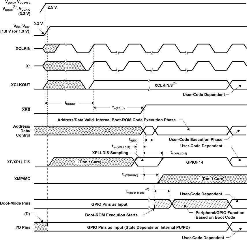
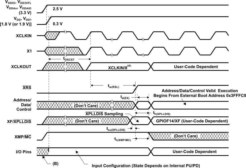
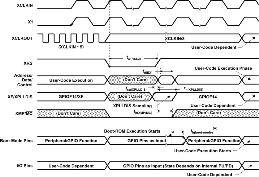
Table 5-3 Reset (XRS) Timing Requirements(1)
| MIN | NOM | MAX | UNIT | |||
|---|---|---|---|---|---|---|
| tw(RSL1) | Pulse duration, stable XCLKIN to XRS high | 8tc(CI) | cycles | |||
| tw(RSL2) | Pulse duration, XRS low | Warm reset | 8tc(CI) | cycles | ||
| tw(WDRS) | Pulse duration, reset pulse generated by watchdog | 512tc(CI) | cycles | |||
| td(EX) | Delay time, address/data valid after XRS high | 32tc(CI) | cycles | |||
| tOSCST(2) | Oscillator start-up time | 1 | 10 | ms | ||
| tsu(XPLLDIS) | Setup time for XPLLDIS pin | 16tc(CI) | cycles | |||
| th(XPLLDIS) | Hold time for XPLLDIS pin | 16tc(CI) | cycles | |||
| th(XMP/MC) | Hold time for XMP/MC pin | 16tc(CI) | cycles | |||
| th(boot-mode) | Hold time for boot-mode pins | 2520tc(CI)(3) | cycles | |||
(1) If external oscillator/clock source are used, reset time has to be low at least for 1 ms after VDD reaches 1.5 V.
(2) Dependent on crystal/resonator and board design.
(3) The boot ROM reads the password locations. Therefore, this timing requirement includes the wakeup time for flash. See the TMS320x281x DSP Boot ROM Reference Guide and the TMS320x281x DSP System Control and Interrupts Reference Guide for further information.

A. VDDAn – VDDA1/VDDA2 and AVDDREFBG
B. Upon power up, SYSCLKOUT is XCLKIN/2 if the PLL is enabled. Since both the XTIMCLK and CLKMODE bits in the XINTCNF2 register come up with a reset state of 1, SYSCLKOUT is further divided by 4 before it appears at XCLKOUT. This explains why XCLKOUT = XCLKIN/8 during this phase.
C. After reset, the Boot ROM code executes instructions for 1260 SYSCLKOUT cycles (SYSCLKOUT = XCLKIN/2) and then samples BOOT Mode pins. Based on the status of the Boot Mode pin, the boot code branches to destination memory or boot code function in ROM. The BOOT Mode pins should be held high/low for at least 2520 XCLKIN cycles from boot ROM execution time for proper selection of Boot modes.
If Boot ROM code executes after power-on conditions (in debugger environment), the Boot code execution time is based on the current SYSCLKOUT speed. The SYSCLKOUT will be based on user environment and could be with or without PLL enabled.
If Boot ROM code executes after power-on conditions (in debugger environment), the Boot code execution time is based on the current SYSCLKOUT speed. The SYSCLKOUT will be based on user environment and could be with or without PLL enabled.
D. The state of the GPIO pins is undefined (that is, they could be input or output) until the 1.8-V (or 1.9-V) supply reaches at least 1 V and 3.3-V supply reaches 2.5 V.
Figure 5-7 Power-on Reset in Microcomputer Mode (XMP/MC = 0) (See Note D) 
A. Upon power up, SYSCLKOUT is XCLKIN/2 if the PLL is enabled. Since both the XTIMCLK and CLKMODE bits in the XINTCNF2 register come up with a reset state of 1, SYSCLKOUT is further divided by 4 before it appears at XCLKOUT. This explains why XCLKOUT = XCLKIN/8 during this phase.
B. The state of the GPIO pins is undefined (that is, they could be input or output) until the 1.8-V (or 1.9-V) supply reaches at least 1 V and 3.3-V supply reaches 2.5 V.
Figure 5-8 Power-on Reset in Microprocessor Mode (XMP/MC = 1) 
A. After reset, the Boot ROM code executes instructions for 1260 SYSCLKOUT cycles (SYSCLKOUT = XCLKIN/2) and then samples BOOT Mode pins. Based on the status of the Boot Mode pin, the boot code branches to destination memory or boot code function in ROM. The BOOT Mode pins should be held high/low for at least 2520 XCLKIN cycles from boot ROM execution time for proper selection of Boot modes.
If Boot ROM code executes after power-on conditions (in debugger environment), the Boot code execution time is based on the current SYSCLKOUT speed. The SYSCLKOUT will be based on user environment and could be with or without PLL enabled.
Figure 5-9 Warm Reset in Microcomputer Mode If Boot ROM code executes after power-on conditions (in debugger environment), the Boot code execution time is based on the current SYSCLKOUT speed. The SYSCLKOUT will be based on user environment and could be with or without PLL enabled.
 Figure 5-10 Effect of Writing Into PLLCR Register