JAJSFY0C August 2018 – December 2018 TMUX1208 , TMUX1209
PRODUCTION DATA.
- 1 特長
- 2 アプリケーション
- 3 概要
- 4 改訂履歴
- 5 Device Comparison Table
- 6 Pin Configuration and Functions
-
7 Specifications
- 7.1 Absolute Maximum Ratings
- 7.2 ESD Ratings
- 7.3 Recommended Operating Conditions
- 7.4 Thermal Information
- 7.5 Electrical Characteristics (VDD = 5 V ±10 %)
- 7.6 Electrical Characteristics (VDD = 3.3 V ±10 %)
- 7.7 Electrical Characteristics (VDD = 1.8 V ±10 %)
- 7.8 Electrical Characteristics (VDD = 1.2 V ±10 %)
- 7.9 Typical Characteristics
- 8 Detailed Description
- 9 Application and Implementation
- 10Power Supply Recommendations
- 11Layout
- 12デバイスおよびドキュメントのサポート
- 13メカニカル、パッケージ、および注文情報
パッケージ・オプション
メカニカル・データ(パッケージ|ピン)
サーマルパッド・メカニカル・データ
発注情報
6 Pin Configuration and Functions
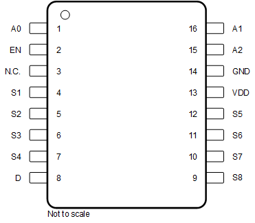
TMUX1208: PW Package
16-Pin TSSOP
Top View

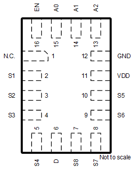
TMUX1208: RSV Package
16-Pin QFN
Top View

Pin Functions TMUX1208
| PIN | TYPE(1) | DESCRIPTION | ||
|---|---|---|---|---|
| NAME | TSSOP | UQFN | ||
| A0 | 1 | 15 | I | Address line 0. Controls the switch configuration as shown in Table 1. |
| EN | 2 | 16 | I | Active high logic input. When this pin is low, all switches are turned off. When this pin is high, the A[2:0] address inputs determine which switch is turned on. |
| N.C. | 3 | 1 | Not Connected | Not Connected |
| S1 | 4 | 2 | I/O | Source pin 1. Can be an input or output. |
| S2 | 5 | 3 | I/O | Source pin 2. Can be an input or output. |
| S3 | 6 | 4 | I/O | Source pin 3. Can be an input or output. |
| S4 | 7 | 5 | I/O | Source pin 4. Can be an input or output. |
| D | 8 | 6 | I/O | Drain pin. Can be an input or output. |
| S8 | 9 | 7 | I/O | Source pin 8. Can be an input or output. |
| S7 | 10 | 8 | I/O | Source pin 7. Can be an input or output. |
| S6 | 11 | 9 | I/O | Source pin 6. Can be an input or output. |
| S5 | 12 | 10 | I/O | Source pin 5. Can be an input or output. |
| VDD | 13 | 11 | P | Positive power supply. This pin is the most positive power-supply potential. For reliable operation, connect a decoupling capacitor ranging from 0.1 µF to 10 µF between VDD and GND. |
| GND | 14 | 12 | P | Ground (0 V) reference |
| A2 | 15 | 13 | I | Address line 2. Controls the switch configuration as shown in Table 1. |
| A1 | 16 | 14 | I | Address line 1. Controls the switch configuration as shown in Table 1. |
(1) I = input, O = output, I/O = input and output, P = power
TMUX1209: PW Package
16-Pin TSSOP
Top View
TMUX1209: RSV Package
16-Pin QFN
Top View
Pin Functions TMUX1209
| PIN | TYPE(1) | DESCRIPTION | ||
|---|---|---|---|---|
| NAME | TSSOP | UQFN | ||
| A0 | 1 | 15 | I | Address line 0. Controls the switch configuration as shown in Table 2. |
| EN | 2 | 16 | I | Active high logic input. When this pin is low, all switches are turned off. When this pin is high, the A[1:0] address inputs determine which switch is turned on. |
| N.C. | 3 | 1 | Not Connected | Not Connected |
| S1A | 4 | 2 | I/O | Source pin 1A. Can be an input or output. |
| S2A | 5 | 3 | I/O | Source pin 2A. Can be an input or output. |
| S3A | 6 | 4 | I/O | Source pin 3A. Can be an input or output. |
| S4A | 7 | 5 | I/O | Source pin 4A. Can be an input or output. |
| DA | 8 | 6 | I/O | Drain pin A. Can be an input or output. |
| DB | 9 | 7 | I/O | Drain pin B. Can be an input or output. |
| S4B | 10 | 8 | I/O | Source pin 4B. Can be an input or output. |
| S3B | 11 | 9 | I/O | Source pin 3B. Can be an input or output. |
| S2B | 12 | 10 | I/O | Source pin 2B. Can be an input or output. |
| S1B | 13 | 11 | I/O | Source pin 1B. Can be an input or output. |
| VDD | 14 | 12 | P | Positive power supply. This pin is the most positive power-supply potential. For reliable operation, connect a decoupling capacitor ranging from 0.1 µF to 10 µF between VDD and GND. |
| GND | 15 | 13 | P | Ground (0 V) reference |
| A1 | 16 | 14 | I | Address line 1. Controls the switch configuration as shown in Table 2. |
(1) I = input, O = output, I/O = input and output, P = power