SLOS841B September 2013 – January 2015 TPA3131D2 , TPA3132D2
PRODUCTION DATA.
- 1 Features
- 2 Applications
- 3 Description
- 4 Revision History
- 5 Pin Configuration and Functions
- 6 Specifications
-
7 Detailed Description
- 7.1 Overview
- 7.2 Functional Block Diagram
- 7.3
Feature Description
- 7.3.1 Gain Setting and Master and Slave
- 7.3.2 Input Impedance
- 7.3.3 Start-up/Shutdown Operation
- 7.3.4 PLIMIT Operation
- 7.3.5 GVDD Supply
- 7.3.6 BSPx and BSNx Capacitors
- 7.3.7 Differential Inputs
- 7.3.8 Device Protection System
- 7.3.9 DC Detect Protection
- 7.3.10 Short-Circuit Protection and Automatic Recovery Feature
- 7.3.11 Thermal Protection
- 7.3.12 Efficiency: LC Filter Required with the Traditional Class-D Modulation Scheme
- 7.3.13 Ferrite Bead Filter Considerations
- 7.3.14 When to Use an Output Filter for EMI Suppression
- 7.3.15 AM Avoidance EMI Reduction
- 7.4 Device Functional Modes
- 8 Applications and Implementation
- 9 Power Supply Recommendations
- 10Layout
- 11Device and Documentation Support
- 12Mechanical, Packaging, and Orderable Information
パッケージ・オプション
メカニカル・データ(パッケージ|ピン)
- RHB|32
サーマルパッド・メカニカル・データ
- RHB|32
発注情報
1 Features
- Supports Multiple Output Configurations
- 2 × 4 W into a 8-Ω BTL Load at 7.4 V (TPA3131D2)
- 2 × 25 W into a 8-Ω BTL Load at 19 V (TPA3132D2)
- Wide Voltage Range: 4.5 V to 26 V
- Automotive Load-Dump Compliant
- Efficient Class-D Operation
- >90% Power Efficiency Combined With Low Idle Loss for Heat Sink free Operation
- Advanced Modulation Schemes
- Multiple Switching Frequencies
- AM Avoidance
- Master and Slave Synchronization
- Up to 1.2-MHz Switching Frequency
- Feedback Power Stage Architecture With High PSRR Reduces PSU Requirements
- Programmable Power Limit
- Differential and Single-Ended Inputs
- Stereo and Mono Mode With Single-Filter Mono Configuration
- Single Power Supply Reduces Component Count
- Integrated Self-Protection Circuits Including Overvoltage, Undervoltage, Overtemperature, DC-Detect, and Short Circuit With Error Reporting
- Thermally Enhanced Package
- 32-Pin VQFN Pad-Down
- –40°C to 85°C Ambient Temperature Range
2 Applications
- Laptop Computers and Ultrabooks
- Flatpanel TV
- Consumer Audio Applications
3 Description
The TPA313xD2 are efficient, stereo digital amplifier power stages for driving speakers with up to 2x42W/4Ω peak power. TPA3131/32D2 operates heatsink-free with cooling to PCB through the bottom side PowerPAD™ with sustained output power from 2 × 4 W / 8 Ω (TPA3131D2) to 2 × 25 W / 8 Ω (TPA3132D2).
The TPA313xD2 advanced oscillator/PLL circuit employs a multiple switching frequency option to avoid AM interferences; this is achieved together with an option of Master and Slave synchronization, making it possible to synchronize multiple devices.
The TPA313xD2 are fully protected against faults with short-circuit protection and thermal protection as well as overvoltage, undervoltage, and DC protection. Faults are reported back to the processor to prevent devices from being damaged during overload conditions.
For feature compatible devices see: PowerPAD up device 2 × 50-W TPA3116D2, PowerPAD down 2 × 15-W TPA3130D2 and 2 × 30-W TPA3118D2.
Device Information(1)
| PART NUMBER | PACKAGE | BODY SIZE (NOM) |
|---|---|---|
| TPA3131D2 | VQFN (32) | 5.00 mm × 5.00 mm |
| TPA3132D2 |
- For all available packages, see the orderable addendum at the end of the datasheet.
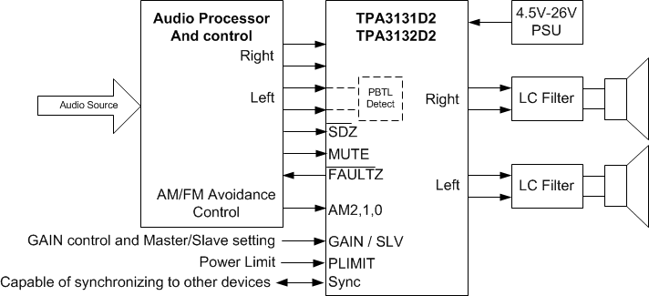
Simplified Application Circuit