SLOS367E August 2003 – November 2015 TPA6211A1
PRODUCTION DATA.
- 1 Features
- 2 Applications
- 3 Description
- 4 Revision History
- 5 Device Comparison Table
- 6 Pin Configuration and Functions
- 7 Specifications
- 8 Parameter Measurement Information
- 9 Detailed Description
-
10Application and Implementation
- 10.1 Application Information
- 10.2
Typical Application
- 10.2.1 Design Requirements
- 10.2.2 Detailed Design Procedure
- 10.2.3 Application Curves
- 10.3 System Examples
- 11Power Supply Recommendations
- 12Layout
- 13Device and Documentation Support
- 14Mechanical, Packaging, and Orderable Information
パッケージ・オプション
デバイスごとのパッケージ図は、PDF版データシートをご参照ください。
メカニカル・データ(パッケージ|ピン)
- DGN|8
- DRB|8
サーマルパッド・メカニカル・データ
発注情報
1 Features
- Designed for Wireless or Cellular Handsets and PDAs
- 3.1 W Into 3 Ω From a 5-V Supply at
THD = 10% (Typ) - Low Supply Current: 4 mA Typ at 5 V
- Shutdown Current: 0.01 μA Typ
- Fast Startup With Minimal Pop
- Only Three External Components
- Improved PSRR (–80 dB) and Wide Supply Voltage (2.5 V to 5.5 V) for Direct Battery Operation
- Fully Differential Design Reduces RF
Rectification - –63 dB CMRR Eliminates Two Input
Coupling Capacitors
2 Applications
- Ideal for Wireless Handsets, PDAs, and
Notebook Computers
3 Description
The TPA6211A1 is a 3.1-W mono fully-differential amplifier designed to drive a speaker with at least 3-Ω impedance while consuming only 20 mm2 total printed-circuit board (PCB) area in most applications. The device operates from 2.5 V to 5.5 V, drawing only 4 mA of quiescent supply current. The TPA6211A1 is available in the space-saving
3-mm × 3-mm SON (DRB) and the 8-pin MSOP-PowerPAD™ (DGN) packages.
Features like –80 dB supply voltage rejection from
20 Hz to 2 kHz, improved RF rectification immunity, small PCB area, and a fast startup with minimal pop makes the TPA6211A1 ideal for PDA and smart phone applications.
Device Information(1)
| PART NUMBER | PACKAGE | BODY SIZE (NOM) |
|---|---|---|
| TPA6211A1 | MSOP-PowerPAD (8) | 3.00 mm × 3.00 mm |
| SON (8) | 3.00 mm × 3.00 mm |
- For all available packages, see the orderable addendum at the end of the data sheet.
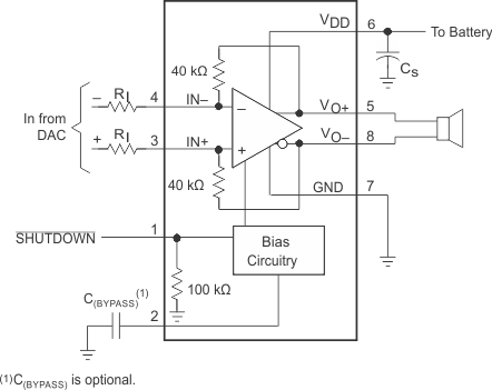
Application Circuit
