SLLSE19F December 2009 – July 2016 TPD12S015
PRODUCTION DATA.
- 1 Features
- 2 Applications
- 3 Description
- 4 Revision History
- 5 Pin Configuration and Functions
-
6 Specifications
- 6.1 Absolute Maximum Ratings
- 6.2 ESD Ratings
- 6.3 Recommended Operating Conditions
- 6.4 Thermal Information
- 6.5 Electrical Characteristics: ICC
- 6.6 Electrical Characteristics: High-Speed ESD Lines: Dx, CLK
- 6.7 Electrical Characteristics: DC-DC Converter
- 6.8 Electrical Characteristics: Passive Components
- 6.9 Electrical Characteristics: Voltage Level Shifter: SCL, SDA Lines (x_A/x_B Ports)
- 6.10 Electrical Characteristics: Voltage Level Shifter: CEC Lines (x_A/x_B Ports)
- 6.11 Electrical Characteristics: Voltage Level Shifter: HPD Line (x_A/x_B Ports)
- 6.12 Electrical Characteristics: LS_OE, CT_CP_HPD
- 6.13 Electrical Characteristics: I/O Capacitance
- 6.14 Switching Characteristics
- 6.15 Switching Characteristics: Voltage Level Shifter: SCL, SDA Lines (x_A & x_B ports); VCCA = 1.2 V
- 6.16 Switching Characteristics: Voltage Level Shifter: CEC Line (x_A & x_B ports); VCCA = 1.2 V
- 6.17 Switching Characteristics: Voltage Level Shifter: HPD Line (x_A & x_B ports); VCCA = 1.2 V
- 6.18 Switching Characteristics: Voltage Level Shifter: SCL, SDA Lines (x_A & x_B ports); VCCA = 1.5 V
- 6.19 Switching Characteristics: Voltage Level Shifter: CEC Line (x_A & x_B ports); VCCA = 1.5 V
- 6.20 Switching Characteristics: Voltage Level Shifter: HPD Line (x_A & x_B ports); VCCA = 1.5 V
- 6.21 Switching Characteristics: Voltage Level Shifter: SCL, SDA Lines (x_A & x_B ports); VCCA = 1.8 V
- 6.22 Switching Characteristics: Voltage Level Shifter: CEC Line (x_A & x_B ports); VCCA = 1.8 V
- 6.23 Switching Characteristics: Voltage Level Shifter: HPD Line (x_A & x_B ports); VCCA = 1.8 V
- 6.24 Switching Characteristics: Voltage Level Shifter: SCL, SDA Lines (x_A & x_B ports); VCCA = 2.5 V
- 6.25 Switching Characteristics: Voltage Level Shifter: CEC Line (x_A & x_B ports); VCCA = 2.5 V
- 6.26 Switching Characteristics: Voltage Level Shifter: HPD Line (x_A & x_B ports); VCCA = 2.5 V
- 6.27 Switching Characteristics: Voltage Level Shifter: SCL, SDA Lines (x_A & x_B ports); VCCA = 3.3 V
- 6.28 Switching Characteristics: Voltage Level Shifter: CEC Line (x_A & x_B ports); VCCA = 3.3 V
- 6.29 Switching Characteristics: Voltage Level Shifter: HPD Line (x_A & x_B ports); VCCA = 3.3 V
- 6.30 Typical Characteristics
- 7 Parameter Measurement Information
- 8 Detailed Description
- 9 Application and Implementation
- 10Power Supply Recommendations
- 11Layout
- 12Device and Documentation Support
- 13Mechanical, Packaging, and Orderable Information
1 Features
- HDMI 1.3 and HDMI 1.4 Data Rate
- HDMI High-Speed Differential Signals –3-dB Bandwidth Exceeds 6.4 Gbps
- Excellent Matching Capacitance (0.05 pF) in Each Differential Signal Pair
- Internal Boost Converter to Generate 5 V From a 2.3-V to 5.5-V Battery Voltage
- HDMI Minimum Current Limit and Short-Circuit Protection at 5VOUT Pin
- Flexible Power-Saving Modes Through Separate Control Pins
- Auto-Direction Sensing Level Shifting in the CEC, SDA, and SCL Lines Drive up to 750-pF Load
- Seamless Type C and Type D Connector Routing With Flow-Through Pin Mapping
- IEC 61000-4-2 (Level 4) System Level ESD Compliance
- Integrated IOFF and Backdrive Current Protection
- Space-Saving 1.6-mm × 2.8-mm DSBGA (YFF) Package
2 Applications
- Smart Phones
- Multimedia Phones
- Digital Camcorders
- Digital Still Cameras
- Portable Game Consoles
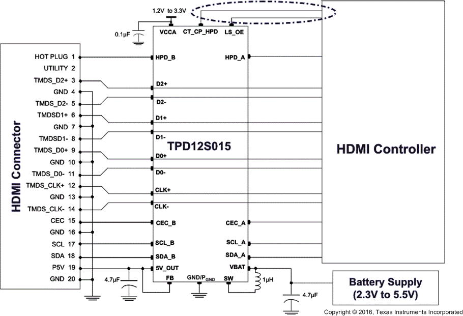
Typical System Diagram

3 Description
The TPD12S015 device is an integrated HDMI ESD solution. The device pin mapping matches the HDMI Type C and Type D connector with four differential pairs. This device offers eight low-capacitance ESD clamps, allowing HDMI 1.3 or 1.4 data rates. The integrated ESD clamps and resistors provide good matching between each differential signal pair, which allows an advantage over discrete ESD clamp solutions where variations between ESD clamps degrade the differential signal quality.
The TPD12S015 provides a regulated 5-V output (5VOUT) for sourcing the HDMI power line. The regulated 5-V output supplies up to 55 mA to the HDMI receiver. The control of 5VOUT and the hot plug detect (HPD) circuitry is independent of the LS_OE control signal and is controlled by the CT_CP_HPD pin. This independent control enables the detection scheme (5VOUT + HPD) to be active before enabling the HDMI link.
There are three noninverting, bidirectional translation circuits for the SDA, SCL, and CEC lines. Each have a common power rail (VCCA) on the A side from 1.1 V to 3.6 V . On the B side, the SCL_B and SDA_B each have an internal 1.75-kΩ pullup connected to the regulated 5-V rail (5VOUT). The SCL and SDA pins meet the I2C specification and drive up to 750-pF loads. The CEC_B pin has an internal 27-kΩ pullup to an internal 3.3-V supply.
The HPD_B port has a glitch filter to avoid false detection due to the bouncing while inserting the HDMI plug.
The TPD12S015 provides IEC61000-4-2 (Level 4) ESD protection. This device is offered in a space-saving 1.6-mm × 2.8-mm wafer-level chip scale package [DSBGA (YFF)] with a 0.4-mm pitch.
Device Information(1)
| PART NUMBER | PACKAGE | BODY SIZE (NOM) |
|---|---|---|
| TPD12S015 | DSBGA (28) | 1.56 mm × 2.76 mm |
- For all available packages, see the orderable addendum at the end of the data sheet.
4 Revision History
Changes from E Revision (June 2013) to F Revision
- Added ESD Ratings table, Thermal Information table, Feature Description section, Device Functional Modes, Application and Implementation section, Power Supply Recommendations section, Layout section, Device and Documentation Support section, and Mechanical, Packaging, and Orderable Information sectionGo
Changes from D Revision (April 2012) to E Revision
- Updated test IOH and IOL test conditions for VOHA, VOLA, and VOHBGo
- Updated test IOH and IOL test conditions for VOHA, VOLA, and VOHBGo
Changes from C Revision (November 2010) to D Revision
- Changed VIH MAX value for CT_CP_HPD, LS_OE parameter from VCCA to 3.6.Go
Changes from B Revision (July 2010) to C Revision