SLLSEK0A December 2014 – February 2015 TPD6F002-Q1
PRODUCTION DATA.
- 1 Features
- 2 Applications
- 3 Description
- 4 Simplified Schematic
- 5 Revision History
- 6 Pin Configuration and Functions
- 7 Specifications
- 8 Detailed Description
- 9 Application and Implementation
- 10Power Supply Recommendations
- 11Layout
- 12Device and Documentation Support
- 13Mechanical, Packaging, and Orderable Information
パッケージ・オプション
メカニカル・データ(パッケージ|ピン)
- DSV|12
サーマルパッド・メカニカル・データ
- DSV|12
発注情報
7 Specifications
7.1 Absolute Maximum Ratings(1)
over operating free-air temperature range (unless otherwise noted)| MIN | MAX | UNIT | |||
|---|---|---|---|---|---|
| VIO | IO to GND | 5.75 | V | ||
| TJ | Junction temperature | 125 | °C | ||
| Tstg | Storage temperature range | –65 | 150 | °C | |
(1) Stresses beyond those listed under "absolute maximum ratings" may cause permanent damage to the device. These are stress ratings only, and functional operation of the device at these or any other conditions beyond those indicated in the operational sections of the specifications is not implied. Exposure to absolute maximum rated conditions for extended periods may affect device reliability.
7.2 ESD Ratings
| VALUE | UNIT | ||||
|---|---|---|---|---|---|
| V(ESD) | Electrostatic discharge | Human body model (HBM), per AEC Q100-002, all pins(1) | ±10 | kV | |
| Charged device model (CDM), per AEC Q101-005, all pins | ±1.5 | ||||
| IEC 61000-4-2 Contact Discharge | ±20 | ||||
| IEC 61000-4-2 Air-Gap Discharge | ±30 | ||||
(1) AEC Q100-002 indicates HBM stressing is done in accordance with the ANSI/ESDA/JEDEC JS-001 specification.
7.3 Recommended Operating Conditions
over operating free-air temperature range (unless otherwise noted)| MIN | NOM | MAX | UNIT | ||
|---|---|---|---|---|---|
| VIO | Input pin voltage | 0 | 5.5 | V | |
| TA | Operating free-air temperature | -40 | 125 | °C | |
7.4 Thermal Information
| THERMAL METRIC(1) | TPD6F002-Q1 | UNIT | |
|---|---|---|---|
| DSV | |||
| 12 PINS | |||
| RθJA | Junction-to-ambient thermal resistance | 120.7 | °C/W |
| RθJC(top) | Junction-to-case (top) thermal resistance | 104.4 | |
| RθJB | Junction-to-board thermal resistance | 78.5 | |
| ψJT | Junction-to-top characterization parameter | 13.0 | |
| ψJB | Junction-to-board characterization parameter | 77.7 | |
| RθJC(bot) | Junction-to-case (bottom) thermal resistance | 66.5 | |
(1) For more information about traditional and new thermal metrics, see the IC Package Thermal Metrics application report, SPRA953.
7.5 Electrical Characteristics
TA = –40°C to 125°C (Unless otherwise noted)| PARAMETER | TEST CONDITIONS | MIN | TYP(1) | MAX | UNIT | |
|---|---|---|---|---|---|---|
| VBR | DC breakdown voltage | IIO = 10 μA | 6 | V | ||
| R | Resistance | VIN = 3.3 V, IIn-to-out = 1mA | 85 | 100 | 115 | Ω |
| C | Capacitance (C1 or C2) | VIO = 2.5 V | 17 | pF | ||
| IIO | Channel leakage current | VIO = 3.3 V | 1 | 20 | nA | |
| fC | Cut-off frequency | ZSOURCE = 50 Ω, ZLOAD = 50 Ω | 100 | MHz | ||
(1) Typical values are at TA = 25°C.
7.6 Typical Characteristics
TA = 25°C unless otherwise noted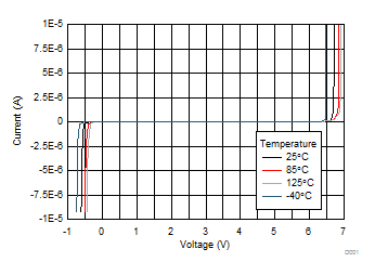 Figure 1. DC Voltage-Current Sweep across Input, Output Pins
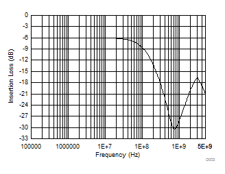 Figure 3. Typical Insertion-loss Characteristics
 (DC Bias = 0 V, 50 Ω Environment)
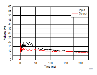 Figure 5. +8-kV IEC Waveform
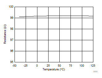 Figure 2. Series Resistance vs Temperature
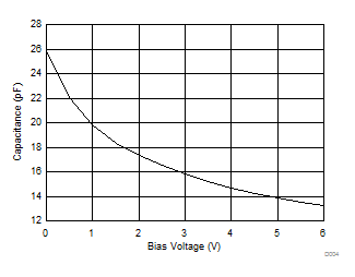 Figure 4. Capacitance (C1 or C2) vs. Bias Voltage
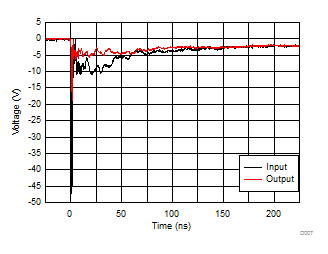 Figure 6. -8-kV IEC Waveform