SLIS167 August 2015 TPIC2050
PRODUCTION DATA.
- 1 Features
- 2 Applications
- 3 Description
- 4 Revision History
- 5 Description (continued)
- 6 Pin Configuration and Functions
- 7 Specifications
-
8 Detailed Description
- 8.1 Overview
- 8.2 Functional Block Diagram
- 8.3 Feature Description
- 8.4 Device Functional Modes
- 8.5 Programming
- 8.6
Register Maps
- 8.6.1 Register State Transition
- 8.6.2 DAC Register (12-Bit Write Only)
- 8.6.3 Control Register (8-Bit Read/Write)
- 8.6.4
Detailed Description of Registers
- 8.6.4.1 REG01 12-Bit DAC for Tilt (offset = 01h) [reset = ]
- 8.6.4.2 REG02 12-Bit DAC for Focus (offset = 02h) [reset = ]
- 8.6.4.3 REG03 12-Bit DAC for Tracking (offset = 03h) [reset = ]
- 8.6.4.4 REG04 12-Bit DAC for Sled1 (offset = 04h) [reset = ]
- 8.6.4.5 REG05 12-Bit DAC for Sled2 (offset = 05h) [reset = ]
- 8.6.4.6 REG06 12-Bit DAC for Stepping1 (offset = 06h) [reset = ]
- 8.6.4.7 REG07 12-Bit DAC for Stepping2 (offset = 07h) [reset = ]
- 8.6.4.8 REG08 12-Bit DAC for Spindle (offset = 08h) [reset = ]
- 8.6.4.9 REG09 12-Bit DAC for Load (offset = 09h) [reset = ]
- 8.6.4.10 REG0A 12-Bit DAC for Laser Diode Driver (offset = 0Ah) [reset = ]
- 8.6.4.11 REG70 8-Bit Control Register for DriverEna (offset = 70h) [reset = ]
- 8.6.4.12 REG71 8-Bit Control Register for FuncEna (offset = 71h) [reset = ]
- 8.6.4.13 REG72 8-Bit Control Register for ACTCfg (offset = 72h) [reset = ]
- 8.6.4.14 REG73 8-Bit Control Register for Parm0 (offset = 73h) [reset = ]
- 8.6.4.15 REG74 8-Bit Control Register for SIFCfg (offset = 74h) [reset = ]
- 8.6.4.16 REG75 8-Bit Control Register for Parm1 (offset = 75h) [reset = ]
- 8.6.4.17 REG76 8-Bit Control Register for WriteEna (offset = 76h) [reset = ]
- 8.6.4.18 REG77 8-Bit Control Register for ClrReg (offset = 77h) [reset = ]
- 8.6.4.19 REG78 8-Bit Control Register for ActTemp (offset = 78h) [reset = ]
- 8.6.4.20 REG79 8-Bit Control Register for UVLOMon (offset = 79h) [reset = ]
- 8.6.4.21 REG7A 8-Bit Control Register for TSDMon (offset = 7Ah) [reset = ]
- 8.6.4.22 REG7B 8-Bit Control Register for OCPMon (offset = 7Bh) [reset = ]
- 8.6.4.23 REG7C 8-Bit Control Register for TempMon (offset = 7Ch) [reset = ]
- 8.6.4.24 REG7E 8-Bit Control Register for Version (offset = 7Eh) [reset = ]
- 8.6.4.25 REG7F 8-Bit Control Register for Status (offset = 7Fh) [reset = ]
- 8.6.4.26 REG61 8-Bit Control Register for SPM1 (offset = 61h) [reset = ]
- 8.6.4.27 REG62 8-Bit Control Register for SPM2 (offset = 62h) [reset = ]
- 8.6.4.28 REG6B 8-Bit Control Register for DisProt (offset = 6Bh) [reset = ]
- 8.6.4.29 REG6C 8-Bit Control Register for STPCfg (offset = 6Ch) [reset = ]
- 8.6.4.30 REG6E 8-Bit Control Register for UtilCfg (offset = 6Eh) [reset = ]
- 8.6.4.31 REG6F 8-Bit Control Register for MonitorSet (offset = 6Fh) [reset = ]
-
9 Application and Implementation
- 9.1
Application Information
- 9.1.1 Voltage Monitoring
- 9.1.2 Spindle Motor Driver Operating Sequence
- 9.1.3 Auto Short Brake Function
- 9.1.4 Spindle PWM Control
- 9.1.5 Spindle Driver Current Limiting Circuit
- 9.1.6 Sled Driver Part
- 9.1.7 Stepping Driver Part
- 9.1.8 Focus/Track/Tilt Driver Part
- 9.1.9 Load Driver Part
- 9.1.10 End Detect Function
- 9.1.11 Load Tray Lock Detect Function
- 9.1.12 Three-Beam Laser Diode Driver
- 9.1.13 Monitor Signal on GPOUT
- 9.1.14 Example Timing of Target Control System
- 9.2 Typical Application
- 9.1
Application Information
- 10Power Supply Recommendations
- 11Layout
- 12Device and Documentation Support
- 13Mechanical, Packaging, and Orderable Information
パッケージ・オプション
メカニカル・データ(パッケージ|ピン)
- DFD|56
サーマルパッド・メカニカル・データ
- DFD|56
発注情報
9 Application and Implementation
NOTE
Information in the following applications sections is not part of the TI component specification, and TI does not warrant its accuracy or completeness. TI’s customers are responsible for determining suitability of components for their purposes. Customers should validate and test their design implementation to confirm system functionality.
9.1 Application Information
9.1.1 Voltage Monitoring
Power faults are reported in the UVLOMon register. Each UVLOMon bit initializes to 0 upon a cold power up. After a fault is detected, the appropriate fault bit is latched high. Writing to the RST_ERRFLG (REG77) clears all UVLOMon bits. Table 39 summarizes the power device faults and actions.
Table 39. Power Fault Monitor
| FAULT TYPE | LATCHED REGISTER | POR | CRITERIA | DRIVER OUTPUT AT DETECTION | |||||
|---|---|---|---|---|---|---|---|---|---|
| SPM | SLED | LOAD | STEP | ACT | LDD | ||||
| P5V under voltage | UVLO_P5V | Yes | <3.7 V | Hi-Z | |||||
| Internal 3.3-V under voltage | UVLO_INT3P3 | Yes | <2.7 V | Hi-Z | |||||
| P12V under voltage | UVLO_P12V | Yes(1) | <8.4 V | Hi-Z | |||||
| SIOV under voltage | UVLO_SIOV | Yes | <2.0 V | Hi-Z | |||||
| P5V over voltage | OVP_P5V | >6.2 V | Hi-Z | ||||||
| P12V over voltage | OVP_P12V | >14.9 V | Hi-Z | — | — | — | |||
9.1.2 Spindle Motor Driver Operating Sequence
When the VSPM is set to a positive DAC code, it enters into acceleration mode. Initial position sense (IS) mode then operates, as the start-up circuits offer the start-up pattern sequence to the driver, then switch to spin-up mode by detecting the rotor position using the BEMF signal from the spindle motor coil.
The spin-down and brake function are also controlled by the DAC value VSPM. When it has set the brake command to the VSPM, the driver goes into active-brake mode, then switches to short-brake mode in slow revolution speed, and then stops automatically. EXOR of a three-phase signal comprises the FG signal and is output from the XFG pin as shown in Figure 49.
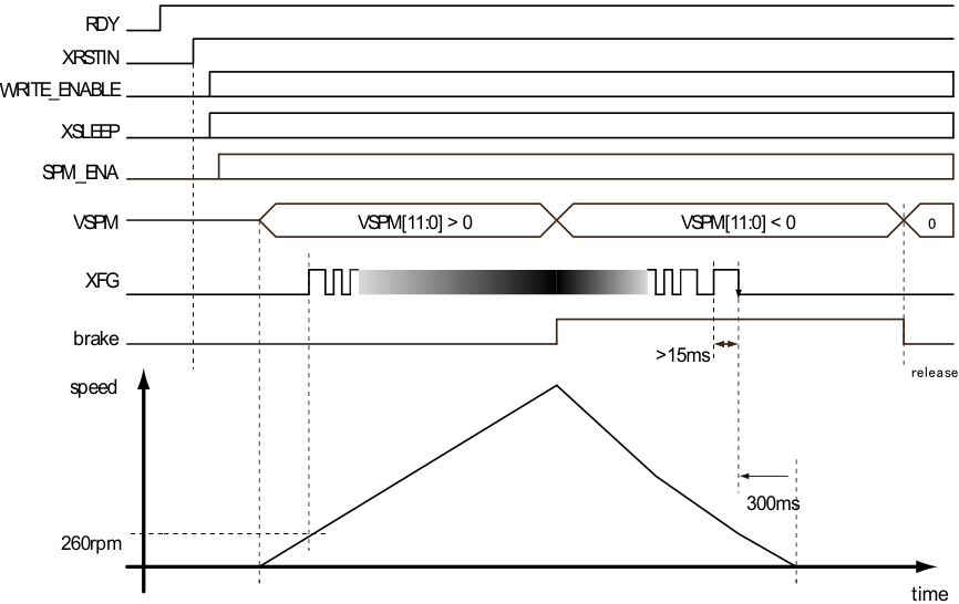 Figure 49. Spindle Operating Sequence
Use the down-edge of the FG signal for monitoring FG frequency.
Short brake mode asserts after 300 ms if the FG signal stays L-level in deceleration.
This value is the nominal number of using a 12-poles motor.
The internal circuit starts 800 µs (typical) after the RDY pin changes to 'H'. Recommended marginal delay value is 1 ms.
9.1.3 Auto Short Brake Function
The TPIC2050 provides an auto short brake function that selects a brake mode automatically by motor speed. Auto short brake includes two modes: short brake and active brake. If a value of 0xF90 or less is set to the VSPM, the brake mode automatically changes at rotation speed. This function enables low-power consumption and silent braking. Figure 50 shows the relation between brake mode and speed. The over-speed protect function suspends the SPM driver output at 15000 or more revolutions.
Table 40. Brake Mode
| VSPM[11:0] | MODE | APPROXIMATE ROTATION SPEED (RPM)(1) | |||
|---|---|---|---|---|---|
| 11500 | 11500 TO 5600 | 5600 TO 4000 | 4000 TO 0 | ||
| 0x000 to 0xFDD | Manual | 2-phase short brake | |||
| 0xFDC to 0xF90 | Manual | Active brake | |||
| 0xF8F to 0xADB | Auto short | Free run | 3-phase short Brake(2) | Active brake | |
| 0xADA to 0x800 | Auto short | Free run | 3-phase short brake(3) | Active brake | |
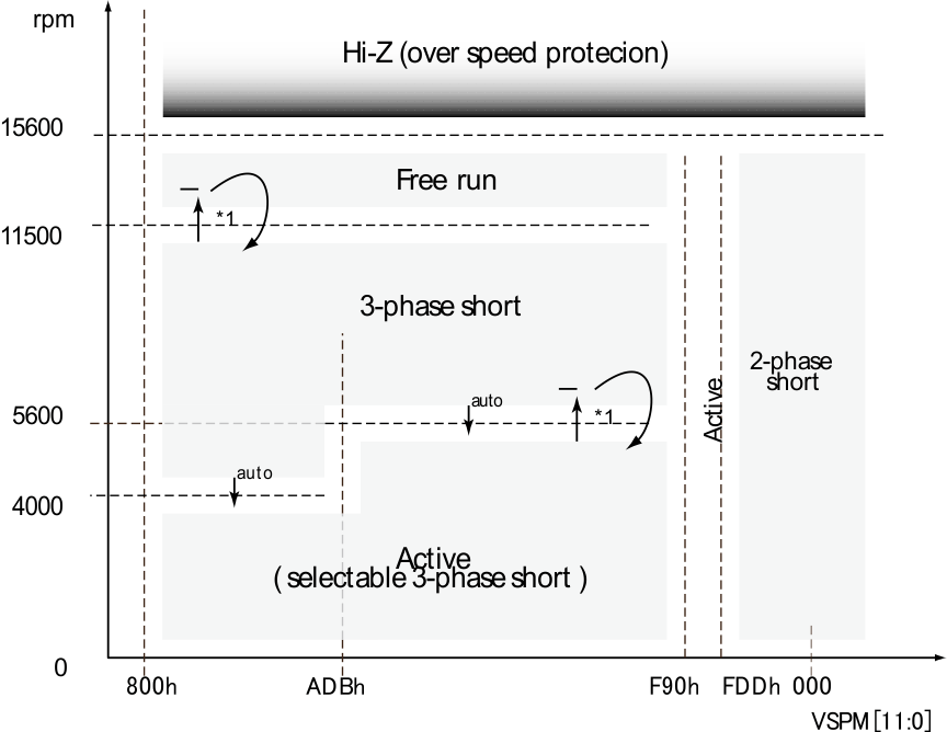
Brake mode will change to specific mode at the threshold speed after it reaches a speed about 15% higher than a threshold speed.
NOTE:
These speed values are the nominal number of using a 12-pole motor. In applying to a 16-pole motor, the rotation speed becomes 75% of indicated rpm values.9.1.4 Spindle PWM Control
The output PWM duty of the spindle is controlled by the DAC code (VSPM). The gain in acceleration setting is always 14 times, but the maximum output is restricted to P12V voltage. A dead band with an output = 0 exists in the width between ±0x52 focusing on zero.
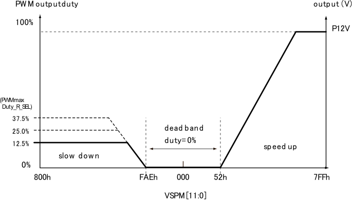 Figure 51. Spindle PWM Control
9.1.5 Spindle Driver Current Limiting Circuit
The current limit circuit monitors the RCS voltage at the ICOM pin and limits the output current by reducing the PWM duty when detecting overcurrent conditions.
9.1.6 Sled Driver Part
The sled driver outputs the PWM pulse set as DAC code (VSLDx) with current feedback. The maximum output is restricted to 880 mA at 0x7FF and 0x800. A dead band with an output = 0 exists in the width of ±0x33 focusing on zero.
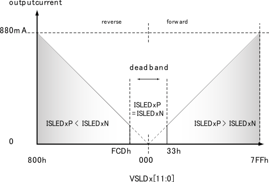 Figure 52. Sled Output Current
Both outputs of SLED1/2 are 'H' when the input code is in the dead band.
9.1.7 Stepping Driver Part
The step driver outputs the PWM pulse, set as an 8-bit DAC code (VSTPx) using VSTP[11:4]. There is no feedback monitor for output. The pulse width is output according to the P5V power supply voltage.
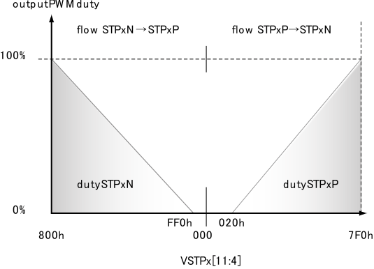 Figure 53. Step Output Duty
9.1.8 Focus/Track/Tilt Driver Part
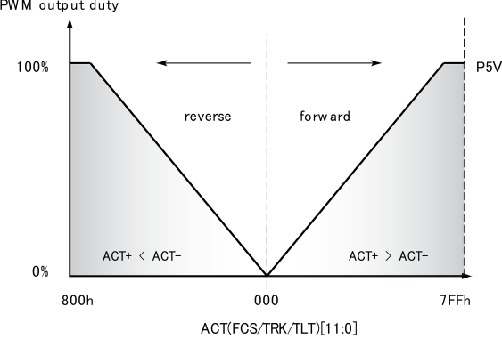 Figure 54. FCS/TRK/TLT Output Duty
9.1.9 Load Driver Part
The load driver outputs the voltage with the voltage feedback corresponding to the input DAC value. This channel has power voltage compensation, and is thus suited for slot-in type load control. This channel becomes active exclusively to other actuator channels. The load driver is shared with the TRK driver.
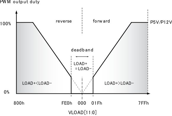 Figure 55. Load Output Duty
9.1.10 End Detect Function
This device has end position detection for the sled and collimator lens. This function eliminates the position switch at the PUH inner and collimator lens end positions. This function is enabled by ENDDET_ENA = 1, setting the object actuator (ENDDET_SEL = 00: for sled / ENDDET_SEL = 01: for step). When this function is enabled, internal logic detects the sled out zero-cross point, then the internal BEMF detect circuit measures the BEMF level of the stepping motor. There are four threshold levels. If the BEMF is lower than the selected threshold, the device recognizes the motor at stop and sets the ENDDET bit to 1. The ENDDET bit is then cleared at the BEMF voltage exceed threshold.
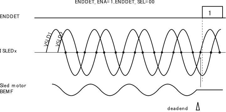 Figure 56. Timing of Sled End Detection
For the purpose of getting the correct stepping motor BEMF, choose a control frequency higher than 110 Hz (440 pps). This control frequency depends on the stepping motor characteristics.
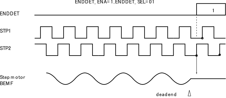 Figure 57. Timing of Step End Detection
The recommended control speed is around 1200 pps for getting the correct BEMF level. This depends on the stepping motor characteristic. Evaluate your condition appropriately.
9.1.11 Load Tray Lock Detect Function
The tray lock detect function detects an inserted obstacle when the tray opens and closes, using the load motor BEMF. Adjusting TRAY_LOCKDET [2:0] (REG75) by the characteristic of a motor is required for an optimal threshold level. The designer can set a threshold level from 100 to 400 mA, with a 50-mA step, using TRAY_LOCKDET.
Observe the lock detection by reading the ENDDET (REG7F) flag where ENDDET_SEL = 2 or 3 is set.
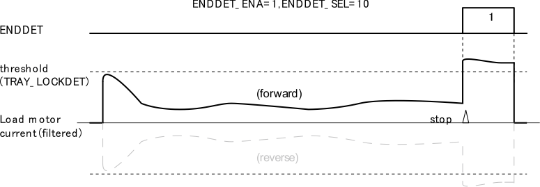 Figure 58. Load Tray Lock Detect
9.1.12 Three-Beam Laser Diode Driver
The device has a circuit for the three-beam laser diode drivers containing Blu-ray™. The output is chosen with LDD_MSEL (REG71), and the LD drive current is outputted by input 11-bit DAC code to VLDD[10:0] and VLDDIN with analog input. The change in analog mode and digital mode is set up by LDD_AMODE (REG74). The MSB of VLDD is the sign bit and is ignored if it set to 1. All output, including BD, DVD, and CD, has an internal pulldown 3 kΩ.
The mode change delay circuit and LVP are integrated to prevent a rush of current when the mode changes. When the LDD mode is changed, VLDD<10:0> is cleared to 0 to prevent the selected laser diode from breaking, as LDD sets the current value according to each kind.
Table 41. LDD Mode
| LDD_MSEL[1:0] | ENABLE | CURRENT OUTPUT |
|---|---|---|
| 11 | BD | ILDD_BD |
| 10 | DVD | ILDD_DVD |
| 01 | CD | ILDD_CD |
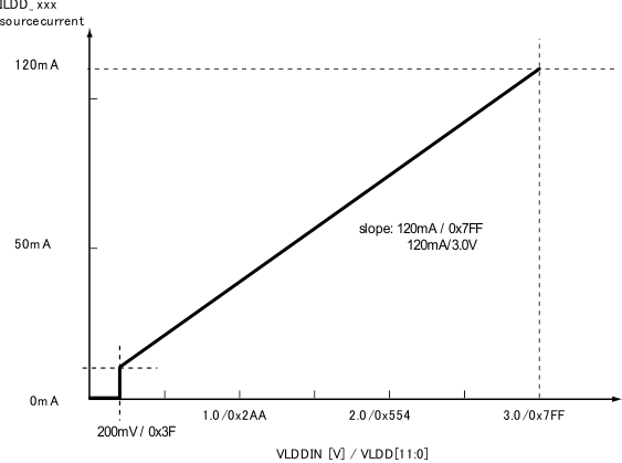 Figure 59. VLDD vs Output Average Current
9.1.13 Monitor Signal on GPOUT
The device can output a specific signal to the GPOUT pin. To output a signal, choose a signal from REG6F by enabling it first, then enabling GPOUT_ENA. When two or more signals are set for GPOUT, the output is a logical sum.
9.1.14 Example Timing of Target Control System
The TPIC2050 is designed to meet the requirements for updating control data in 400 kHz. Table 42 lists examples of the control system parameters. It takes 0.51 µs to transmit a 16-bit data packet to the TPIC2050 with a 35-MHz SCLK. Therefore, DSP can be sent in four packets at a 400-kHz interval. If the SCLK is lower than 28.8 MHz, the user must reduce the packet quantity to less than three. For example, the Focus/Truck command updates every 2.5 µs (400 kHz), and is able to send another two kinds of packets in this same slot. Figure 60 shows an example of the control timing when using the TPIC2050.
Table 42. Example Timing of Target Control System
| SIGNAL | BIT | UPDATE CYCLE (kHz) |
|---|---|---|
| Focus | 12 | 400 |
| Track | 12 | 400 |
| Tilt | 12 | 100 |
| Sled1 | 10 | 100 |
| Sled2 | 10 | 100 |
| Spindle | 12 | 100 |
| Load | 12 | — |
| Step1 | 8 | 40 |
| Step2 | 8 | 40 |
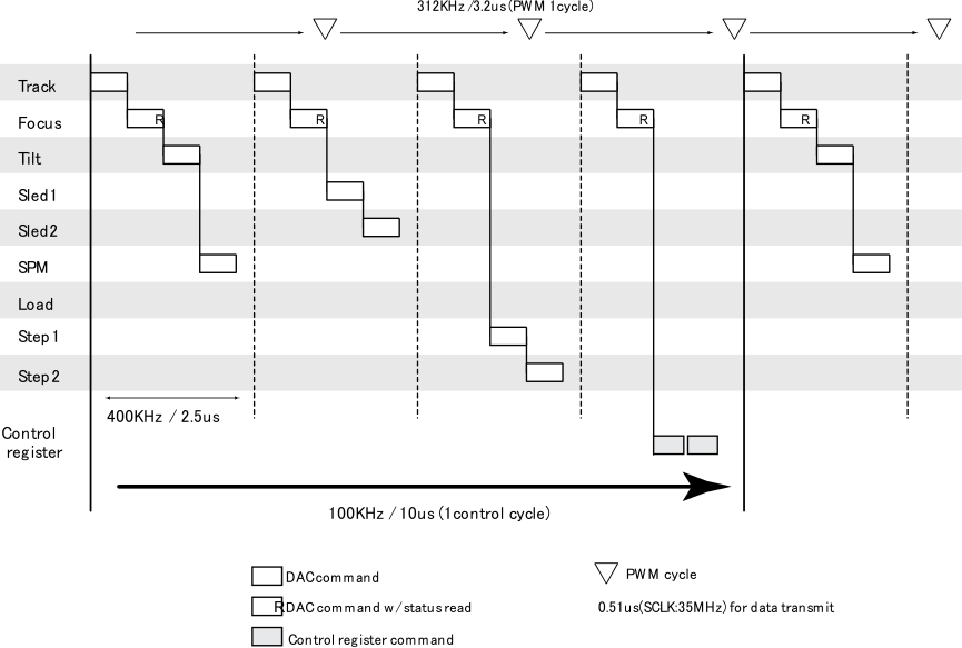 Figure 60. Example DAC Control
9.2 Typical Application
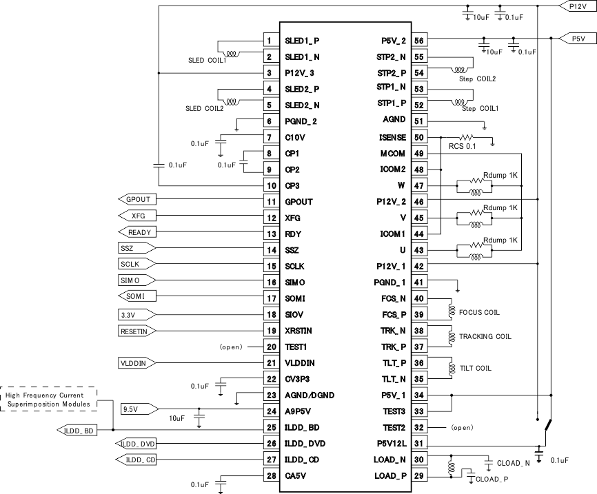 Figure 61. Example Application Circuit
9.2.1 Design Requirements
To begin the design process, determine the following:
- Motor configuration: The user can use all motor channels or part of them.
- Usage for ILDD: BD, DVD, or CD
- RDY pin can be connected to Host CPU, then Host CPU can know the power supply status of TPIC2050.
9.2.2 Detailed Design Procedure
After power up on 5-V and 12-V supply, register can be changed following way and enabling motors.
- Set WRITE_ENABLE = 1 on REG76 via SPI.
- Set XSLEEP = 1 at REG70
- Enable motor channel by ENA_XXX bits on REG70
- Change the DAC settings for the motor on REG01-0B. Then, output channels start driving load.
9.2.3 Application Curves
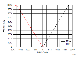 Figure 62. TRK Driver: DAC Code vs Output On Duty
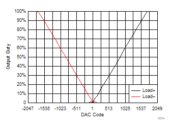 Figure 63. Load Driver: DAC Code vs Output On Duty