SLIS167 August 2015 TPIC2050
PRODUCTION DATA.
- 1 Features
- 2 Applications
- 3 Description
- 4 Revision History
- 5 Description (continued)
- 6 Pin Configuration and Functions
- 7 Specifications
-
8 Detailed Description
- 8.1 Overview
- 8.2 Functional Block Diagram
- 8.3 Feature Description
- 8.4 Device Functional Modes
- 8.5 Programming
- 8.6
Register Maps
- 8.6.1 Register State Transition
- 8.6.2 DAC Register (12-Bit Write Only)
- 8.6.3 Control Register (8-Bit Read/Write)
- 8.6.4
Detailed Description of Registers
- 8.6.4.1 REG01 12-Bit DAC for Tilt (offset = 01h) [reset = ]
- 8.6.4.2 REG02 12-Bit DAC for Focus (offset = 02h) [reset = ]
- 8.6.4.3 REG03 12-Bit DAC for Tracking (offset = 03h) [reset = ]
- 8.6.4.4 REG04 12-Bit DAC for Sled1 (offset = 04h) [reset = ]
- 8.6.4.5 REG05 12-Bit DAC for Sled2 (offset = 05h) [reset = ]
- 8.6.4.6 REG06 12-Bit DAC for Stepping1 (offset = 06h) [reset = ]
- 8.6.4.7 REG07 12-Bit DAC for Stepping2 (offset = 07h) [reset = ]
- 8.6.4.8 REG08 12-Bit DAC for Spindle (offset = 08h) [reset = ]
- 8.6.4.9 REG09 12-Bit DAC for Load (offset = 09h) [reset = ]
- 8.6.4.10 REG0A 12-Bit DAC for Laser Diode Driver (offset = 0Ah) [reset = ]
- 8.6.4.11 REG70 8-Bit Control Register for DriverEna (offset = 70h) [reset = ]
- 8.6.4.12 REG71 8-Bit Control Register for FuncEna (offset = 71h) [reset = ]
- 8.6.4.13 REG72 8-Bit Control Register for ACTCfg (offset = 72h) [reset = ]
- 8.6.4.14 REG73 8-Bit Control Register for Parm0 (offset = 73h) [reset = ]
- 8.6.4.15 REG74 8-Bit Control Register for SIFCfg (offset = 74h) [reset = ]
- 8.6.4.16 REG75 8-Bit Control Register for Parm1 (offset = 75h) [reset = ]
- 8.6.4.17 REG76 8-Bit Control Register for WriteEna (offset = 76h) [reset = ]
- 8.6.4.18 REG77 8-Bit Control Register for ClrReg (offset = 77h) [reset = ]
- 8.6.4.19 REG78 8-Bit Control Register for ActTemp (offset = 78h) [reset = ]
- 8.6.4.20 REG79 8-Bit Control Register for UVLOMon (offset = 79h) [reset = ]
- 8.6.4.21 REG7A 8-Bit Control Register for TSDMon (offset = 7Ah) [reset = ]
- 8.6.4.22 REG7B 8-Bit Control Register for OCPMon (offset = 7Bh) [reset = ]
- 8.6.4.23 REG7C 8-Bit Control Register for TempMon (offset = 7Ch) [reset = ]
- 8.6.4.24 REG7E 8-Bit Control Register for Version (offset = 7Eh) [reset = ]
- 8.6.4.25 REG7F 8-Bit Control Register for Status (offset = 7Fh) [reset = ]
- 8.6.4.26 REG61 8-Bit Control Register for SPM1 (offset = 61h) [reset = ]
- 8.6.4.27 REG62 8-Bit Control Register for SPM2 (offset = 62h) [reset = ]
- 8.6.4.28 REG6B 8-Bit Control Register for DisProt (offset = 6Bh) [reset = ]
- 8.6.4.29 REG6C 8-Bit Control Register for STPCfg (offset = 6Ch) [reset = ]
- 8.6.4.30 REG6E 8-Bit Control Register for UtilCfg (offset = 6Eh) [reset = ]
- 8.6.4.31 REG6F 8-Bit Control Register for MonitorSet (offset = 6Fh) [reset = ]
-
9 Application and Implementation
- 9.1
Application Information
- 9.1.1 Voltage Monitoring
- 9.1.2 Spindle Motor Driver Operating Sequence
- 9.1.3 Auto Short Brake Function
- 9.1.4 Spindle PWM Control
- 9.1.5 Spindle Driver Current Limiting Circuit
- 9.1.6 Sled Driver Part
- 9.1.7 Stepping Driver Part
- 9.1.8 Focus/Track/Tilt Driver Part
- 9.1.9 Load Driver Part
- 9.1.10 End Detect Function
- 9.1.11 Load Tray Lock Detect Function
- 9.1.12 Three-Beam Laser Diode Driver
- 9.1.13 Monitor Signal on GPOUT
- 9.1.14 Example Timing of Target Control System
- 9.2 Typical Application
- 9.1
Application Information
- 10Power Supply Recommendations
- 11Layout
- 12Device and Documentation Support
- 13Mechanical, Packaging, and Orderable Information
パッケージ・オプション
メカニカル・データ(パッケージ|ピン)
- DFD|56
サーマルパッド・メカニカル・データ
- DFD|56
発注情報
7 Specifications
7.1 Absolute Maximum Ratings
over operating free-air temperature range (unless otherwise noted) (1)| MIN | MAX | UNIT | |||
|---|---|---|---|---|---|
| 5-V supply voltage P5V | 6 | V | |||
| 12-V supply voltage P12V | 15 | ||||
| 9.5-V supply voltage A9P5V | 15 | ||||
| Load supply P5V12 voltage | 15 | ||||
| Spindle output peak voltage | 15 | ||||
| Spindle output current | 2.5 | A | |||
| Spindle output peak current, (PW ≤ 2 ms, Duty ≤ 30%) | 3.5 | ||||
| Sled output peak current | 1.0 | ||||
| Focus/tracking/tilt driver output peak current | 1.0 | ||||
| Load driver output peak current | 1.0 | ||||
| Laser diode driver output peak current | 247(3) | mA | |||
| Input/output voltage | –0.3 | VCC + 0.3 | V | ||
| Power dissipation(2) | 1344 | mW | |||
| Operating temperature | –20 | 75 | °C | ||
| Lead temperature 1.6 mm from case for 10 s | 260 | ||||
| Tstg | Storage temperature | –60 | 150 | ||
(1) Stresses beyond those listed under Absolute Maximum Ratings may cause permanent damage to the device. These are stress ratings only, which do not imply functional operation of the device at these or any other conditions beyond those indicated under Recommended Operating Conditions. Exposure to absolute-maximum-rated conditions for extended periods may affect device reliability.
(2) A lower RθJC is attainable if the exposed pad is connected to a large copper ground plane. RθJC and RθJA are values for 56-pin TSSOP without a exposed heat slug (HSL) on bottom. Actual thermal resistance would be better than the above values.
(3) The LDD output time of the maximum current should maintain 25% or less of the xsleep total ON time.
7.2 ESD Ratings
| VALUE | UNIT | |||
|---|---|---|---|---|
| V(ESD) | Electrostatic discharge | Human-body model (HBM), per ANSI/ESDA/JEDEC JS-001(1) | ±2000 | V |
| Charged-device model (CDM), per JEDEC specification JESD22-C101(2) | ±500 | |||
(1) JEDEC document JEP155 states that 500-V HBM allows safe manufacturing with a standard ESD control process.
(2) JEDEC document JEP157 states that 250-V CDM allows safe manufacturing with a standard ESD control process.
7.3 Recommended Operating Conditions
over operating free-air temperature range (unless otherwise noted)| MIN | NOM | MAX | UNIT | ||
|---|---|---|---|---|---|
| P5V | Operating supply voltage (apply for P5V) | 4.5 | 5.0 | 5.5 | V |
| P12V | Driver 12-V supply voltage (apply for P12V(1)) | 10.8 | 12.0 | 13.2 | |
| A9P5V | Power supply laser diode for BD (apply for A9P5V) | 7.65 | 9.5 | 10.45 | |
| P5V12L | Load operating supply voltage (apply for P5V12L) | 4.5 | 5.0 | 5.5 | |
| 10.8 | 12.0 | 13.2 | |||
| VSIOV | SIOV voltage | 3.0 | 3.3 | 36 | |
| Tope | Operating temperature range | –20 | 25 | 75 | °C |
| Fck | SCLK frequency | 30 | 33.8688 | 35 | MHz |
| VSIFH | SIMO, SSZ, SCLK pin 'H' level input voltage range | 2.2 | SIOV + 0.2 | V | |
| VSIFL | SIMO, SSZ, SCLK pin 'L' level input voltage range | –0.2 | 0.8 | ||
| VIHB | XRSTIN pin 'H' level input voltage | 2.2 | P5V + 0.1 | ||
| VILB | XRSTIN pin 'L' level input voltage range | –0.1 | 0.8 | ||
| ISPMOA | Spindle output average current U,V,W Total) | 0.5 | 1.7 | A | |
| ISPMO | Spindle output current | 1.7 | |||
| ISLDOA | Sled output average current | 0.25 | 0.8 | ||
| IACTOA | Focus/ tracking/ tilt/ loading output average current | 0.5 | 0.8 | ||
| ISTPOA | STP output average current | 300 | mA | ||
(1) (P5V = 4.5 to 5.5 V, P12V = 10.8 to 13.2 V, CATA ≈ –20℃ to 75℃, unless otherwise noted)
7.4 Thermal Information
| THERMAL METRIC(1) | TPIC2050 | UNIT | |
|---|---|---|---|
| DFD (HTSSOP) | |||
| 56 PINS | |||
| RθJA | Junction-to-ambient thermal resistance | 16.7 | °C/W |
| RθJC | Junction-to-case thermal resistance | 0.8 | °C/W |
| RθJB | Junction-to-board thermal resistance | 5.1 | °C/W |
| ψJT | Junction-to-top characterization parameter | 0.9 | °C/W |
| ψJB | Junction-to-board characterization parameter | 5.1 | °C/W |
| RθJC(bot) | Junction-to-case (bottom) thermal resistance | 0.9 | °C/W |
(1) For more information about traditional and new thermal metrics, see the Semiconductor and IC Package Thermal Metrics application report, SPRA953.
7.5 Electrical Characteristics
over operating free-air temperature range (unless otherwise noted)| PARAMETER | TEST CONDITIONS | MIN | TYP | MAX | UNIT | |
|---|---|---|---|---|---|---|
| COMMON PART | ||||||
| ISTBY | Standby supply current | Standby mode | 0.6 | 1.2 | mA | |
| VCV3 | CV3P3 output voltage | Iload = 25 mA | 3.1 | 3.3 | 3.4 | V |
| RXM | XRSTIN pulldown resistor | 100 | 200 | 300 | kΩ | |
| RRDY | RDY pullup resistor | 1.5 | 33 | 49.5 | ||
| VRDY | RDY low level output voltage | SIOV = 3.3 V, IOL = –100 µA | 0.3 | V | ||
| RXFG | XFG output resistor | 100 | 200 | 300 | Ω | |
| VXFGH | XFG high-level output voltage | SIOV = 3.3 V, XSLEEP = 1, IOH = 100 µA | SIOV – 0.3 | V | ||
| VXFGL | XFG low-level output voltage | SIOV = 3.3 V, XSLEEP = 1, IOL = 100 µA | 0.3 | |||
| RGPO | GPOUT output resistor | 100 | 200 | 300 | Ω | |
| VGPOH | GPOUT high-level output voltage | SIOV = 3.3 V, XSLEEP = 1, GPOUT_ENA = 1, GPOUT_HL = 1, IOH = 100 µA | SIOV – 0.3 | V | ||
| VGPOL | GPOUT low-level output voltage | SIOV = 3.3 V, XSLEEP = 1, GPOUT_ENA = 1, GPOUT_HL = 0, IOH = 100 µA | 0.3 | |||
| TTSD | Thermal protection on temperature | Design value | 135 | 150 | 165 | °C |
| TSDhys | Thermal protection hysteresis temperature | 5 | 15 | 25 | ||
| Vonvcc | P5V reset on voltage | 3.6 | 3.7 | 3.8 | V | |
| Voffvcc | P5V reset off voltage | 3.8 | 3.9 | 4.0 | V | |
| Vonvcc | P12V reset on voltage | 7.9 | 8.4 | 8.9 | V | |
| Voffcc | P12V reset off voltage | 8.3 | 8.8 | 9.3 | V | |
| VonCV3 | CV3P3 reset on voltage | 2.6 | 2.7 | 2.8 | V | |
| VoffCV3 | CV3P3 reset off voltage | 2.7 | 2.8 | 2.9 | V | |
| VovpPspmOn | OVP predetection voltage (spindle) | 13.4 | 14.1 | 14.8(1) | V | |
| VovpPspmOff | OVP prerelease voltage (spindle) | 13.1 | 13.8 | 14.5(1) | V | |
| VovpspmOn | OVP detection voltage (spindle) | 14.2 | 14.9 | 15.6(1) | V | |
| VovpspmOff | OVP release voltage (spindle) | 13.9 | 14.6 | 15.3(1) | V | |
| VovpOn | OVP detection voltage (except spindle) | 6.0 | 6.2 | 6.4(1) | V | |
| VovpOff | OVP release voltage (except spindle) | 5.8 | 6.0 | 6.2(1) | V | |
| CHARGE PUMP PART | ||||||
| FCHGP | Frequency | XSLEEP = 1 | 132.6 | 156 | 179.4 | kHz |
| VCHGP | Output voltage | Ccp1 = Ccp3 = 0.1 µF Io = –1 mA | 15.6 | 18.5 | 21.4 | V |
| SPINDLE MOTOR DRIVER PART | ||||||
| RttlSPM | Total output resistance high side + low side | IOUT = 500 mA | 0.3 | 0.6 | Ω | |
| VIsns | Spindle current limit reference voltage | 160 | 170 | 180 | mV | |
| VIsnsP | For flash peak current detection | 179 | 194 | 209 | ||
| ResSPM | Resolution | 12 | bit | |||
| VoutSPM | Spindle gain | Magnification to 1.0 inputs | 12.4 | 14.0 | 15.6 | times |
| WidDZSPM | Spindle dead band | Forward | 12h | 52h | 92h | |
| Reverse | –92h | –52h | –12h | |||
| SLED MOTOR DRIVER PART | ||||||
| RttlSLD | Total output resistance high side + low side | P12V = 10.8 to 13.2 V, IO = 500 mA | 1.6 | 2.5 | Ω | |
| ResSLD | Resolution | 10 | bit | |||
| WidDZSLD | Input dead band | Forward | +4h | +33h | +62h | |
| Reverse | –62h | –33h | –4h | |||
| GnSLD | Sled current gain | P5V = 5 V, P12V = 12 V VSLED = 7FFh | 760 | 880 | 1000 | mA |
| VthEdetSLD | END_DET BEMF threshold voltage | ENDDET_SLCT = 0, SLEDENDTH<1:0> = ,SLED Enable | 62 | 124 | 186 | mV |
| FOCUS/TILT/TRACKING DRIVER PART | ||||||
| RttlAct | Each channel total output resistance high side + low side | P5V = 4.5 V to 5.5 V, IO = 500 mA | 0.7 | 1.1 | Ω | |
| ResACT | Resolution | 12 | bit | |||
| VOfstACT | Each channel output offset voltage | DAC_code = 000h | –30 | 0 | 30 | mV |
| GnAct | Each channel voltage gain | Magnification to 1.0 inputs | 4.7 | 6.0 | 7.6 | times |
| LOAD DRIVER PART | ||||||
| RttlLOD | Total output resistance high side + low side | P5V12L = 4.5 to 5.5 V, IO = 500 mA | 1.2 | 1.9 | Ω | |
| P5V12L = 10.8 to 13.2 V, IO = 500 mA | ||||||
| ResLOD | Resolution | 12 | bit | |||
| GnLOD | Voltage gain | P5V12L = 4.5 to 5.5 V | 4.7 | 6.0 | 7.6 | V |
| P5V12L = 10.8 to 13.2 V | 11.1 | 14.0 | 17.6 | |||
| WidDZLOD | Dead band | Forward | 20h | |||
| Reverse | –21h | |||||
| LockDth | Tray lock detect threshold current | P5V12L = 5 V, TRAY_LOCKDET[2:0] = 1 | 80 | 100 | 120 | mA |
| P5V12L = 12 V, TRAY_LOCKDET[2:0] = 1 | 80 | 100 | 120 | |||
| P5V12L = 5 V, TRAY_LOCKDET[2:0] = 2 | 120 | 150 | 180 | |||
| P5V12L = 12 V, TRAY_LOCKDET[2:0] = 2 | 120 | 150 | 180 | |||
| P5V12L = 5 V, TRAY_LOCKDET[2:0] = 3 | 160 | 200 | 240 | |||
| P5V12L = 12 V, TRAY_LOCKDET[2:0] = 3 | 160 | 200 | 240 | |||
| P5V12L = 5 V, TRAY_LOCKDET[2:0] = 4 | 212 | 250 | 287 | |||
| P5V12L = 12 V, TRAY_LOCKDET[2:0] = 4 | 212 | 250 | 287 | |||
| P5V12L = 5 V, TRAY_LOCKDET[2:0] = 5 | 255 | 300 | 345 | |||
| P5V12L = 12 V, TRAY_LOCKDET[2:0] = 5 | 255 | 300 | 345 | |||
| P5V12L = 5 V, TRAY_LOCKDET[2:0] = 6 | 297 | 300 | 345 | |||
| P5V12L = 12 V, TRAY_LOCKDET[2:0] = 6 | 297 | 300 | 345 | |||
| P5V12L = 5 V, TRAY_LOCKDET[2:0] = 7 | 340 | 400 | 460 | |||
| P5V12L = 12 V, TRAY_LOCKDET[2:0] = 7 | 340 | 400 | 460 | |||
| STEPPING MOTOR DRIVER PART | ||||||
| RttlSTP | Total output resistance high side + low side | IO = 100 mA | 1.0 | 1.5 | Ω | |
| ResSTP | Resolution | 8 | bit | |||
| IocpSTP | Overcurrent protection level | 595 | 850 | 1148(1) | mA | |
| tDlyocpSTP | OCP monitor delay time | 0.7 | 1.0 | 1.3(1) | µs | |
| thlocpSTP | OCP hold time | 17 | 25 | 32(1) | ms | |
| VthEdetSTP | END_DET threshold level | ENDDET_SLCT = 1, STPDENDTH<1:0> = 00, STP Enable | 19 | 39 | 59 | mV |
| LDD DRIVER PART | ||||||
| AV(2) | LDD current gain in digital mode VLDD = 0x7FF IUP = 00 |
LDD_MSEL:01(CD), 10(DVD) A9P5V = 7.65 to 10.45 V | 102 | 120 | 138 | mA |
| LDD_MSEL:11(BD) A9P5V = 8.55 to 10.45 V | 102 | 120 | 138 | |||
| LDD_MSEL:11(BD) A9P5V = 7.65 to 8.55 V | 98 | 120 | 141 | |||
| AV(2) | LDD current gain in analog mode VLDDIN input voltage = 3 V IUP = 00 |
LDD_MSEL:01(CD), 10(DVD) A9P5V = 7.65 to 10.45 V | 102 | 120 | 138 | mA |
| LDD_MSEL:11(BD) A9P5V = 8.55 to 10.45 V | 102 | 120 | 138 | |||
| LDD_MSEL:11(BD) A9P5V = 7.65 to 8.55 V | 98 | 120 | 141 | |||
| AV(2)(3) | LDD current gain by IUP setting (digital mode only) LDD_MSEL: 01(CD), 10(DVD) |
VLDD = 0x7FF, LDD_IUP = 00 | 102 | 120 | 138 | mA |
| VLDD = 0, LDD_IUP = 00 | –10 | 0 | 10 | |||
| VLDD = 0x7FF, LDD_IUP = 01 | 119 | 149 | 178 | |||
| VLDD = 0x7FF, LDD_IUP = 10 | 141 | 177 | 212 | |||
| VLDD = 0x7FF, LDD_IUP = 11 | 164 | 206 | 247 | |||
| AV(2)(3) | LDD current gain by IUP setting (digital mode only) LDD_MSEL:11(BD) at A9P5V = 8.55 to 10.45 V |
VLDD = 0x7FF, LDD_IUP = 00 | 102 | 120 | 138 | mA |
| VLDD = 0, LDD_IUP = 00 | –10 | 0 | 10 | |||
| VLDD = 0x7FF, LDD_IUP = 01 | 119 | 149 | 178 | |||
| VLDD = 0x7FF, LDD_IUP = 10 | 141 | 177 | 212 | |||
| VLDD = 0x7FF, LDD_IUP = 011 | 164 | 206 | 247 | |||
| AV(2)(3) | LDD current gain by IUP setting (digital mode only) LDD_MSEL:11(BD) at A9P5V = 7.65 to 8.55 V |
VLDD = 0x7FF, LDD_IUP = 00 | 98 | 120 | 141 | mA |
| VLDD = 0, LDD_IUP = 00 | –10 | 0 | 10 | |||
| VLDD = 0x7FF, LDD_IUP = 01 | 114 | 149 | 183 | |||
| VLDD = 0x7FF, LDD_IUP = 10 | 136 | 177 | 217 | |||
| VLDD = 0x7FF, LDD_IUP = 11 | 158 | 206 | 253 | |||
| ResLDD | LDD current gain | P5V = 4.5 V to 5.5 V, A9P5V = 9.5 V | 11 | bit | ||
| tr | Rise time of ILDD | P5V = 5 V VLDDIN = 0 → 0x7FF 120 mA |
162 | 203 | 243 | µs |
| tf | Fall time of ILDD | P5V = 5 V VLDDIN = 0x7FF → 0 50 mA |
162 | 203 | 243 | |
| IZ | VLDDIN input impedance | 100 | 200 | 300 | kΩ | |
| LDDdbA | Low voltage dead band | 140 | 200 | 260 | mV | |
| LDDdbA | 0x3F | bit | ||||
| THERMOMETER PART | ||||||
| ResTEMP | Resolution | 6 | bit | |||
| Trng | Temperature range | CHIPTEMP[5:0] = 00 | 8 | 15 | 22 | °C |
| CHIPTEMP[5:0] = 3Fh | 155 | 165 | 175 | |||
| FTEMP | Update cycle | 10 | kHz | |||
| ACTUATOR PROTECTION | ||||||
| tintACTTEMP | Update cycle | 26 | ms | |||
| SERIAL PORT VOLTAGE LEVELS | ||||||
| SOMI | High-level output voltage, VOH | IOH = 1 mA | 80% SIOV | V | ||
| SOMI | Low-level output voltage, VOL | IOL = 1 mA | 20% SIOV | V | ||
| SIMO | High-level input voltage, VIH | 70% SIOV | V | |||
| SIMO | Low-level input voltage, VIL | 20% SIOV | V | |||
| tSIMO | Input rise/fall time | 20% ⇔ 80% SIOV | 3.5 | ns | ||
| tSOMI | Output rise/fall time(4) | Cload = 30 pF, 20% ⇔ 80% SIOV | 10 | ns | ||
| RSCLK | Internal pulldown resistance | 100 | 200 | 300 | kΩ | |
| RSSZ | Internal pullup resistance | 100 | 200 | 300 | kΩ | |
(1) These value are protection functions only, and stress beyond those listed under Recommended Operating Conditions may cause permanent damage to the device.
(2) ILDD_BD = 4.5 V, ILDD_CD = 2.1 V ILDD_DVD = 2.1 V
(3) LDD_IUP settings are only for digital mode.
(4) Specified by design
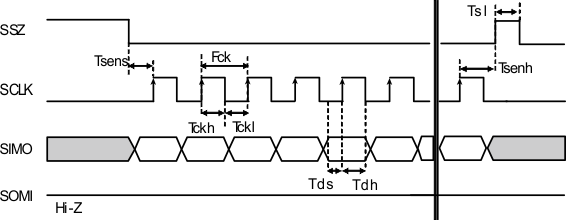
7.6 Serial I/F Write Timing Requirements
| MIN | NOM | MAX | UNIT | |||
|---|---|---|---|---|---|---|
| ƒck | SCLK clock frequency | SIOV = 3.3 V | 35 | MHz | ||
| tckl | SCLK low time | 11 | ns | |||
| tckh | SCLK high time | 11 | ns | |||
| tsens | SSZ setup time | 7 | ns | |||
| tsenh | SSZ hold time | 7 | ns | |||
| tsl | SSZ disable high time | 11 | ns | |||
| tds | SIMO setup time (Write) | 7 | ns | |||
| tdh | SIMO hold time (Write) | 7 | ns | |||
 Figure 1. Serial Port Write Timing
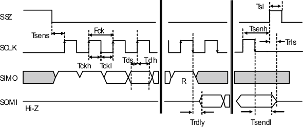
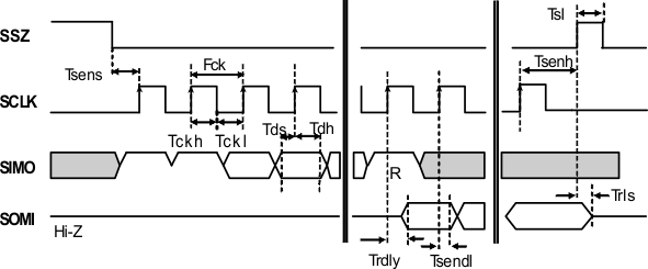
7.7 Serial I/F Read Timing Requirements
| MIN | NOM | MAX | UNIT | |||
|---|---|---|---|---|---|---|
| ƒck | SCLK clock frequency | SIOV = 3.3 V | 35 | MHz | ||
| tckl | SCLK low time | 11 | ns | |||
| tckh | SCLK high time | 11 | ns | |||
| tsens | SSZ setup time | 7 | ns | |||
| tsenh | SSZ hold time | 7 | ns | |||
| tsl | SSZ disable high time | 11 | ns | |||
| tds | SIMO setup time (Write) | 7 | ns | |||
| tdh | SIMO hold time (Write) | 7 | ns | |||
| trdly | SOMI delay time (Read) | CLOAD = 10 pF, SIOV = 3.3 V | 2 | 9 | ns | |
| tsendl | SOMI hold time (Read) | CLOAD = 10 pF, SIOV = 3.3 V | 2 | 9 | ns | |
| trls | SOMI release time (Read) | CLOAD = 10 pF, SIOV = 3.3 V from SSZ rise to SOMI HIZ | 0 | 9 | ns | |
 Figure 2. Serial Port Read Timings
 Figure 3. Serial Port Read Timings (Advanced Read Mode)
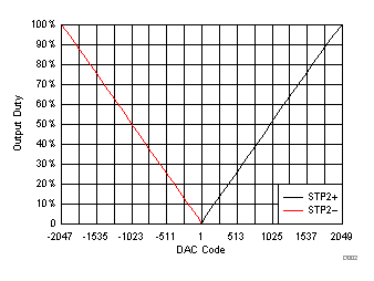
7.8 Typical Characteristics

