SLVSD76C February 2016 – July 2017 TPS22918
PRODUCTION DATA.
- 1 Features
- 2 Applications
- 3 Description
- 4 Revision History
- 5 Pin Configuration and Functions
- 6 Specifications
- 7 Parameter Measurement Information
- 8 Detailed Description
- 9 Application and Implementation
- 10Power Supply Recommendations
- 11Layout
- 12Device and Documentation Support
- 13Mechanical, Packaging, and Orderable Information
1 Features
- Integrated Single Channel Load Switch
- Ambient Operating Temperature: –40°C to +105°C
- Input Voltage Range: 1 V to 5.5 V
- On-Resistance (RON)
- RON = 52 mΩ (typical) at VIN = 5 V
- RON = 53 mΩ (typical) at VIN = 3.3 V
- 2-A Maximum Continuous Switch Current
- Low Quiescent Current
- 8.3 µA (typical) at VIN = 3.3 V
- Low-Control Input-Threshold Enables Use of 1 V or Higher GPIO
- Adjustable Quick-Output Discharge (QOD)
- Configurable Rise Time With CT Pin
- Small SOT23-6 Package (DBV)
- 2.90-mm × 2.80-mm, 0.95-mm Pitch,
1.45 mm Height (with leads)
- 2.90-mm × 2.80-mm, 0.95-mm Pitch,
- ESD Performance Tested per JESD 22
- ±2-kV HBM and ±1-kV CDM
2 Applications
- Industrial Systems
- Set Top Box
- Blood Glucose Meters
- Electronic Point of Sale
3 Description
The TPS22918 is a single-channel load switch with configurable rise time and configurable quick output discharge. The device contains an N-channel MOSFET that can operate over an input voltage range of 1 V to 5.5 V and can support a maximum continuous current of 2 A. The switch is controlled by an on and off input, which is capable of interfacing directly with low-voltage control signals.
The configurable rise time of the device greatly reduces inrush current caused by large bulk load capacitances, thereby reducing or eliminating power supply droop. The TPS22918 features a configurable quick output discharge (QOD) pin, which controls the fall time of the device to allow design flexibility for power down and sequencing.
The TPS22918 is available in a small, leaded SOT-23 package (DBV) which allows visual inspection of solder joints. The device is characterized for operation over the free-air temperature range of –40°C to +105°C.
Device Information (1)
| PART NUMBER | PACKAGE | BODY SIZE (NOM) |
|---|---|---|
| TPS22918 | SOT-23 (6) | 2.90 mm × 1.60 mm |
- For all available packages, see the orderable addendum at the end of the datasheet.
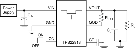
Simplified Schematic

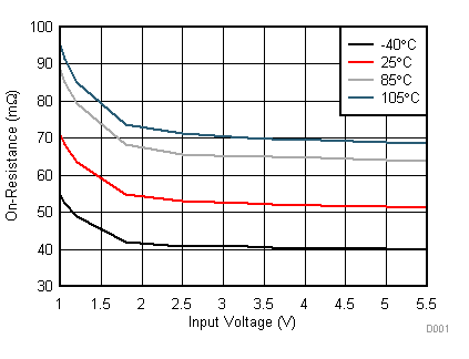
On-Resistance vs Input Voltage
Typical Values
