SLUS599B June 2004 – October 2015 TPS2400
PRODUCTION DATA.
- 1 Features
- 2 Applications
- 3 Description
- 4 Revision History
- 5 Pin Configuration and Functions
- 6 Specifications
- 7 Parameter Measurement Information
- 8 Detailed Description
- 9 Application and Implementation
- 10Power Supply Recommendations
- 11Layout
- 12Device and Documentation Support
- 13Mechanical, Packaging, and Orderable Information
パッケージ・オプション
デバイスごとのパッケージ図は、PDF版データシートをご参照ください。
メカニカル・データ(パッケージ|ピン)
- DBV|5
サーマルパッド・メカニカル・データ
発注情報
9 Application and Implementation
NOTE
Information in the following applications sections is not part of the TI component specification, and TI does not warrant its accuracy or completeness. TI’s customers are responsible for determining suitability of components for their purposes. Customers should validate and test their design implementation to confirm system functionality.
9.1 Application Information
The TPS2400 device provides application flexibility and can be used in many types of systems for load protection.
9.2 Typical Applications
9.2.1 TPS2400 Application
When the TPS2400 disconnects the load from the power supply, the power-supply output-voltage spikes as the stored energy in inductor LS is released. A Zener diode D1 or a small ceramic capacitor can be used to keep the voltage spike at a safe level.
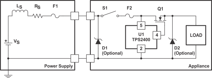 Figure 15. TPS2400 Application Block Diagram
9.2.1.1 Design Requirements
Table 1 shows the parameters for this design example.
Table 1. Design Parameters
| DESIGN PARAMETERS | EXAMPLE VALUE |
|---|---|
| MOSFET Input Capacitance, CG | 2 nF |
| Load Capacitance, CL | 100 uF |
9.2.1.2 Detailed Design Procedure
9.2.1.2.1 Controlling the Load Inrush-Current
Figure 16 is a simplified representation of an appliance with a plug-in power supply (for example, wall adapter). When power is first applied to the load in Figure 16, the large filter capacitor CLOAD acts like a short circuit, producing an immediate inrush-current that is limited by the power-supply output resistance and inductance, RS and LS, respectively. This current can be several orders of magnitude greater than the steady-state load current. The large inrush current can damage power connectors P1 and J1 and power switch S1, and stress components. Increasing the power-supply output resistance and inductance lowers the inrush current. However, the former increases system power-dissipation and the latter decreases connector and switch reliability by encouraging the contacts to arc when they bounce.
 Figure 16. Power-Supply Output Resistance and Inductance Circuit Model
The TPS2400 circuit in Figure 17 limits the inrush current without these draw backs. The TPS2400 device charges the transistor Q1 gate capacitance CG with a 5-µA source when Q1 is commanded to turn on. Transistor Q1 is wired as a source follower so the gate-voltage slew rate and the load-voltage slew rate are identical and equal to

The corresponding inrush current is:

When solving Equation 1 using CG = 2 nF, we get 2500 V/s. Then we can use Equation 2 to approximate the inrush current of 250 mA.
An external capacitor and a series 1-kΩ resistor can be connected to the gate of Q1 and ground to reduce inrush current further. In this case, the parameter CG in Equation 1 and Equation 2 is the sum of the internal and external FET gate capacitance. The 1-kΩ resistor decouples the external gate capacitor, so the TPS2400 device can rapidly turn off transistor Q1 in response to an overvoltage condition.
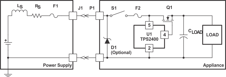 Figure 17. Turnon Voltage Slew Rate Control Using the TPS2400
9.2.1.3 Application Curve
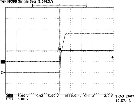 Figure 18. Circuit Start-Up With VIN = 5 V
