JAJS340F November 2008 – August 2016 TPS2552 , TPS2552-1 , TPS2553 , TPS2553-1
PRODUCTION DATA.
- 1 特長
- 2 アプリケーション
- 3 概要
- 4 改訂履歴
- 5 Device Comparison Table
- 6 Pin Configuration and Functions
- 7 Specifications
- 8 Parameter Measurement Information
- 9 Detailed Description
- 10Application and Implementation
- 11Power Supply Recommendations
- 12Layout
- 13デバイスおよびドキュメントのサポート
- 14メカニカル、パッケージ、および注文情報
パッケージ・オプション
メカニカル・データ(パッケージ|ピン)
サーマルパッド・メカニカル・データ
- DRV|6
発注情報
10 Application and Implementation
NOTE
Information in the following applications sections is not part of the TI component specification, and TI does not warrant its accuracy or completeness. TI’s customers are responsible for determining suitability of components for their purposes. Customers should validate and test their design implementation to confirm system functionality.
10.1 Application Information
10.1.1 Constant-Current vs Latch-Off Operation and Impact on Output Voltage
Both the constant-current devices (TPS255x) and latch-off devices (TPS255x-1) operate identically during normal operation, that is, the load current is less than the current-limit threshold and the devices are not limiting current. During normal operation the N-channel MOSFET is fully enhanced, and VOUT = VIN - (IOUT x rDS(on)). The voltage drop across the MOSFET is relatively small compared to VIN, and VOUT ≉ VIN.
Both the constant-current devices (TPS255x ) and latch-off devices (TPS255x-1) operate identically during the initial onset of an overcurrent event. Both devices limit current to the programmed current-limit threshold set to RILIM by operating the N-channel MOSFET in the linear mode. During current-limit operation, the N-channel MOSFET is no longer fully-enhanced and the resistance of the device increases. This allows the device to effectively regulate the current to the current-limit threshold. The effect of increasing the resistance of the MOSFET is that the voltage drop across the device is no longer negligible (VIN ≠ VOUT), and VOUT decreases. The amount that VOUT decreases is proportional to the magnitude of the overload condition. The expected VOUT can be calculated by,
where
For example, if IOS is programmed to 1 A and a 1 Ω overload condition is applied, the resulting VOUT is 1 V.
While both the constant-current devices (TPS255x ) and latch-off devices (TPS255x-1) operate identically during the initial onset of an overcurrent event, they behave differently if the overcurrent event lasts longer than the internal delay de-glitch circuit (7.5-ms typical). The constant-current devices (TPS255x ) assert the FAULT flag after the deglitch period and continue to regulate the current to the current-limit threshold indefinitely. In practical circuits, the power dissipation in the package increases the die temperature above the overtemperature shutdown threshold (135°C minimum), and the device turns off until the die temperature decreases by the hysteresis of the thermal shutdown circuit (10°C typical). The device turns on and continues to thermal cycle until the overload condition is removed. The constant-current devices resume normal operation once the overload condition is removed. The latch-off devices (TPS255x-1) assert the FAULT flag after the deglitch period and immediately turn off the device. The device remains off regardless of whether the overload condition is removed from the output. The latch-off devices remain off and do not resume normal operation until the surrounding system either toggles the enable or cycles power to the device.
10.2 Typical Applications
10.2.1 Two-Level Current-Limit Circuit
Some applications require different current-limit thresholds depending on external system conditions. Figure 24 shows an implementation for an externally controlled, two-level current-limit circuit. The current-limit threshold is set by the total resistance from ILIM to GND (see the Programming the Current-Limit Threshold section). A logic-level input enables or disables MOSFET Q1 and changes the current-limit threshold by modifying the total resistance from ILIM to GND. Additional MOSFET and resistor combinations can be used in parallel to Q1/R2 to increase the number of additional current-limit levels.
NOTE
ILIM must never be driven directly with an external signal.
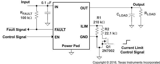 Figure 24. Two-Level Current-Limit Circuit
10.2.1.1 Design Requirements
For this example, use the parameters shown in Table 1.
Table 1. Design Requirements
| PARAMETER | VALUE |
|---|---|
| Input voltage | 5 V |
| Output voltage | 5 V |
| Above a minimum current limit | 1000 mA |
| Below a maximum current limit | 500 mA |
10.2.1.2 Detailed Design Procedures
10.2.1.2.1 Designing Above a Minimum Current Limit
Some applications require that current limiting cannot occur below a certain threshold. For this example, assume that 1 A must be delivered to the load so that the minimum desired current-limit threshold is 1000 mA. Use the IOS equations and Figure 23 to select RILIM.
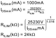
Select the closest 1% resistor less than the calculated value: RILIM = 23.7 kΩ. This sets the minimum current-limit threshold at 1 A . Use the IOS equations, Figure 23, and the previously calculated value for RILIM to calculate the maximum resulting current-limit threshold.
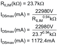
The resulting maximum current-limit threshold is 1172.4 mA with a 23.7-kΩ resistor.
10.2.1.2.2 Designing Below a Maximum Current Limit
Some applications require that current limiting must occur below a certain threshold. For this example, assume that the desired upper current-limit threshold must be below 500 mA to protect an up-stream power supply. Use the IOS equations and Figure 23 to select RILIM.
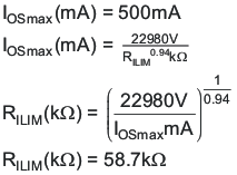
Select the closest 1% resistor greater than the calculated value: RILIM = 59-kΩ. This sets the maximum current-limit threshold at 500 mA . Use the IOS equations, Figure 23, and the previously calculated value for RILIM to calculate the minimum resulting current-limit threshold.
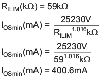
The resulting minimum current-limit threshold is 400.6 mA with a 59-kΩ resistor.
10.2.1.2.3 Accounting for Resistor Tolerance
The previous sections described the selection of RILIM given certain application requirements and the importance of understanding the current-limit threshold tolerance. The analysis focused only on the TPS255x and TPS255x-1 performance and assumed an exact resistor value. However, resistors sold in quantity are not exact and are bounded by an upper and lower tolerance centered around a nominal resistance. The additional RILIM resistance tolerance directly affects the current-limit threshold accuracy at a system level. The following table shows a process that accounts for worst-case resistor tolerance assuming 1% resistor values. Step one follows the selection process outlined in the application examples above. Step two determines the upper and lower resistance bounds of the selected resistor. Step three uses the upper and lower resistor bounds in the IOS equations to calculate the threshold limits. It is important to use tighter tolerance resistors, for example, 0.5% or 0.1%, when precision current limiting is desired.
Table 2. Common RILIM Resistor Selections
| DESIRED NOMINAL CURRENT LIMIT (mA) |
IDEAL RESISTOR (kΩ) |
CLOSEST 1% RESISTOR (kΩ) |
RESISTOR TOLERANCE | ACTUAL LIMITS | |||
|---|---|---|---|---|---|---|---|
| 1% LOW (kΩ) | 1% HIGHT (kΩ) | IOS MIN (mA) | IOS NOM (mA) | IOS MAX (mA) | |||
| 75 | SHORT ILIM to IN | 50.0 | 75.0 | 100.0 | |||
| 120 | 226.1 | 226 | 223.7 | 228.3 | 101.3 | 120.0 | 142.1 |
| 200 | 134.0 | 133 | 131.7 | 134.3 | 173.7 | 201.5 | 233.9 |
| 300 | 88.5 | 88.7 | 87.8 | 89.6 | 262.1 | 299.4 | 342.3 |
| 400 | 65.9 | 66.5 | 65.8 | 67.2 | 351.2 | 396.7 | 448.7 |
| 500 | 52.5 | 52.3 | 51.8 | 52.8 | 448.3 | 501.6 | 562.4 |
| 600 | 43.5 | 43.2 | 42.8 | 43.6 | 544.3 | 604.6 | 673.1 |
| 700 | 37.2 | 37.4 | 37.0 | 37.8 | 630.2 | 696.0 | 770.8 |
| 800 | 32.4 | 32.4 | 32.1 | 32.7 | 729.1 | 800.8 | 882.1 |
| 900 | 28.7 | 28.7 | 28.4 | 29.0 | 824.7 | 901.5 | 988.7 |
| 1000 | 25.8 | 26.1 | 25.8 | 26.4 | 908.3 | 989.1 | 1081.0 |
| 1100 | 23.4 | 23.2 | 23.0 | 23.4 | 1023.7 | 1109.7 | 1207.5 |
| 1200 | 21.4 | 21.5 | 21.3 | 21.7 | 1106.0 | 1195.4 | 1297.1 |
| 1300 | 19.7 | 19.6 | 19.4 | 19.8 | 1215.1 | 1308.5 | 1414.9 |
| 1400 | 18.3 | 18.2 | 18.0 | 18.4 | 1310.1 | 1406.7 | 1517.0 |
| 1500 | 17.0 | 16.9 | 16.7 | 17.1 | 1412.5 | 1512.4 | 1626.4 |
| 1600 | 16.0 | 15.8 | 15.6 | 16.0 | 1512.5 | 1615.2 | 1732.7 |
| 1700 | 15.0 | 15.0 | 14.9 | 15.2 | 1594.5 | 1699.3 | 1819.4 |
10.2.1.2.4 Input and Output Capacitance
Input and output capacitance improves the performance of the device; the actual capacitance must be optimized for the particular application. For all applications, TI recommends placing a 0.1-µF or greater ceramic bypass capacitor between IN and GND as close to the device as possible for local noise de-coupling. This precaution reduces ringing on the input due to power-supply transients. Additional input capacitance may be needed on the input to reduce voltage overshoot from exceeding the absolute maximum voltage of the device during heavy transient conditions. This is especially important during bench testing when long, inductive cables are used to connect the evaluation board to the bench power-supply.
TI recommends placing a high-value electrolytic capacitor on the output pin when large transient currents are expected on the output.
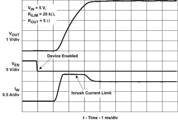
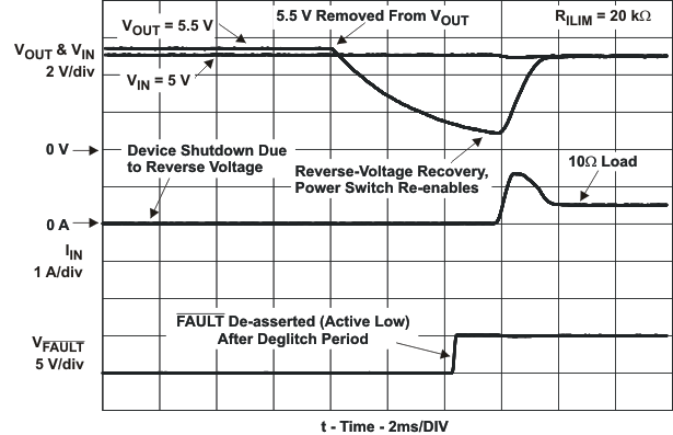
10.2.1.3 Application Curves
10.2.2 Auto-Retry Functionality
Some applications require that an overcurrent condition disables the part momentarily during a fault condition and re-enables after a pre-set time. This auto-retry functionality can be implemented with an external resistor and capacitor. During a fault condition, FAULT pulls low disabling the part. The part is disabled when EN is pulled low, and FAULT goes high impedance allowing CRETRY to begin charging. The part re-enables when the voltage on EN reaches the turnon threshold, and the auto-retry time is determined by the resistor-capacitor time constant. The device continues to cycle in this manner until the fault condition is removed.
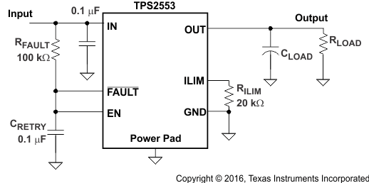 Figure 27. Auto-Retry Functionality
Some applications require auto-retry functionality and the ability to enable or disable with an external logic signal. Figure 28 shows how an external logic signal can drive EN through RFAULT and maintain auto-retry functionality. The resistor-capacitor time constant determines the auto-retry time-out period.
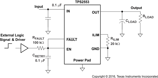 Figure 28. Auto-Retry Functionality With External EN Signal
10.2.2.1 Design Requirements
For this example, use the parameters shown in Table 3.
Table 3. Design Requirements
| PARAMETER | VALUE |
|---|---|
| Input voltage | 5 V |
| Output voltage | 5 V |
| Current | 1200 mA |
10.2.2.2 Detailed Design Procedure
Refer to Programming the Current-Limit Threshold section for the current limit setting. For auto-retry functionality, once FAULT asserted, EN pull low, TPS2553 is disabled, FAULT des-asserted, CRETRY is slowly charged to EN logic high through RFAULT, then enable, after deglitch time, FAULT asserted again. In the event of an overload, TPS2553 cycles and has output average current. ON-time with output current is decided by FAULT deglitch time. OFF-time without output current is decided by RFAULT x CRETRY constant time to EN logic high and ton time. Therefore, set the RFAULT × CRETRY to get the desired output average current during overload.
10.2.3 Typical Application as USB Power Switch
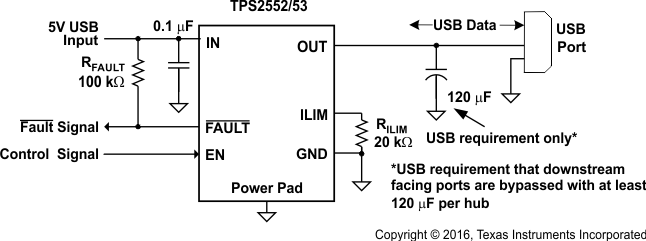 Figure 29. Typical Application as USB Power Switch
10.2.3.1 Design Requirements
For this example, use the parameters shown in Table 4.
Table 4. Design Requirements
| PARAMETER | VALUE |
|---|---|
| Input voltage | 5 V |
| Output voltage | 5 V |
| Current | 1200 mA |
10.2.3.1.1 USB Power-Distribution Requirements
USB can be implemented in several ways regardless of the type of USB device being developed. Several power-distribution features must be implemented.
- SPHs must:
- Current limit downstream ports
- Report overcurrent conditions
- BPHs must:
- Enable or disable power to downstream ports
- Power up at <100 mA
- Limit inrush current (<44 Ω and 10 µF)
- Functions must:
- Limit inrush currents
- Power up at <100 mA
The feature set of the TPS255x and TPS255x-1 meets each of these requirements. The integrated current limiting and overcurrent reporting is required by self-powered hubs. The logic-level enable and controlled rise times meet the need of both input and output ports on bus-powered hubs and the input ports for bus-powered functions.
10.2.3.2 Detailed Design Procedure
10.2.3.2.1 Universal Serial Bus (USB) Power-Distribution Requirements
One application for this device is for current limiting in universal serial bus (USB) applications. The original USB interface was a 12-Mbps or 1.5-Mbps, multiplexed serial bus designed for low-to-medium bandwidth PC peripherals (for example, keyboards, printers, scanners, and mice). As the demand for more bandwidth increased, the USB 2.0 standard was introduced increasing the maximum data rate to 480-Mbps. The four-wire USB interface is conceived for dynamic attach-detach (hot plug-unplug) of peripherals. Two lines are provided for differential data, and two lines are provided for 5-V power distribution.
USB data is a 3.3-V level signal, but power is distributed at 5 V to allow for voltage drops in cases where power is distributed through more than one hub across long cables. Each function must provide its own regulated 3.3 V from the 5-V input or its own internal power supply. The USB specification classifies two different classes of devices depending on its maximum current draw. A device classified as low-power can draw up to 100 mA as defined by the standard. A device classified as high-power can draw up to 500 mA. It is important that the minimum current-limit threshold of the current-limiting power-switch exceed the maximum current-limit draw of the intended application. The latest USB standard must always be referenced when considering the current-limit threshold
The USB specification defines two types of devices as hubs and functions. A USB hub is a device that contains multiple ports for different USB devices to connect and can be self-powered (SPH) or bus-powered (BPH). A function is a USB device that is able to transmit or receive data or control information over the bus. A USB function can be embedded in a USB hub. A USB function can be one of three types included in the list below.
- Low-power, bus-powered function
- High-power, bus-powered function
- Self-powered function
SPHs and BPHs distribute data and power to downstream functions. The TPS255x has higher current capability than required for a single USB port allowing it to power multiple downstream ports.