JAJS340F November 2008 – August 2016 TPS2552 , TPS2552-1 , TPS2553 , TPS2553-1
PRODUCTION DATA.
- 1 特長
- 2 アプリケーション
- 3 概要
- 4 改訂履歴
- 5 Device Comparison Table
- 6 Pin Configuration and Functions
- 7 Specifications
- 8 Parameter Measurement Information
- 9 Detailed Description
- 10Application and Implementation
- 11Power Supply Recommendations
- 12Layout
- 13デバイスおよびドキュメントのサポート
- 14メカニカル、パッケージ、および注文情報
パッケージ・オプション
メカニカル・データ(パッケージ|ピン)
サーマルパッド・メカニカル・データ
- DRV|6
発注情報
7 Specifications
7.1 Absolute Maximum Ratings
over operating free-air temperature range (unless otherwise noted) (1)(2)| MIN | MAX | UNIT | |||
|---|---|---|---|---|---|
| Voltage range on IN, OUT, EN or EN, ILIM, FAULT | –0.3 | 7 | V | ||
| Voltage range from IN to OUT | –7 | 7 | V | ||
| IO | Continuous output current | Internally Limited | |||
| Continuous total power dissipation | See the Thermal Information | ||||
| Continuous FAULT sink current | 0 | 25 | mA | ||
| ILIM source current | 0 | 1 | mA | ||
| TJ | Maximum junction temperature | –40 | 150 | °C | |
| Tstg | Storage temperature | –65 | 150 | °C | |
(1) Stresses beyond those listed under Absolute Maximum Ratings may cause permanent damage to the device. These are stress ratings only, which do not imply functional operation of the device at these or any other conditions beyond those indicated under Recommended Operating Conditions. Exposure to absolute-maximum-rated conditions for extended periods may affect device reliability.
(2) Voltages are referenced to GND unless otherwise noted.
7.2 ESD Ratings
| VALUE | UNIT | ||||
|---|---|---|---|---|---|
| V(ESD) | Electrostatic discharge | Human body model (HBM), per ANSI/ESDA/JEDEC JS-001(1) | ±2000 | V | |
| Charged device model (CDM), per JEDEC specification JESD22-C101(2) | ±500 | ||||
| IEC 61000-4-2 contact discharge(3) | ±8000 | ||||
| IEC 61000-4-2 air-gap discharge(3) | ±15000 | ||||
(1) JEDEC document JEP155 states that 500-V HBM allows safe manufacturing with a standard ESD control process.
(2) JEDEC document JEP157 states that 250-V CDM allows safe manufacturing with a standard ESD control process.
(3) Surges per EN61000-4-2. 1999 applied to output terminals of EVM. These are passing test levels, not failure threshold.
7.3 Recommended Operating Conditions
over operating free-air temperature range (unless otherwise noted)| MIN | NOM | MAX | UNIT | |||
|---|---|---|---|---|---|---|
| VIN | Input voltage, IN | 2.5 | 6.5 | V | ||
| VEN | Enable voltage | TPS2552/52-1 | 0 | 6.5 | V | |
| VEN | Enable voltage | TPS2553/53-1 | 0 | 6.5 | V | |
| VIH | High-level input voltage on EN or EN | 1.1 | V | |||
| VIL | Low-level input voltage on EN or EN | 0.66 | ||||
| IOUT | Continuous output current, OUT | –40 °C ≤ TJ ≤ 125 °C | 0 | 1.2 | A | |
| –40 °C ≤ TJ ≤ 105 °C | 0 | 1.5 | ||||
| RILIM | Current-limit threshold resistor range (nominal 1%) from ILIM to GND | 15 | 232 | kΩ | ||
| IO | Continuous FAULT sink current | 0 | 10 | mA | ||
| Input de-coupling capacitance, IN to GND | 0.1 | µF | ||||
| TJ | Operating virtual junction temperature(1) | IOUT ≤ 1.2 A | –40 | 125 | °C | |
| IOUT ≤ 1.5 A | –40 | 105 | ||||
(1) See Power Dissipation and Junction Temperature for details on how to calculate maximum junction temperature for specific applications and packages.
7.4 Thermal Information
| THERMAL METRIC(1) | TPS2552 | TPS2553 | UNIT | |||
|---|---|---|---|---|---|---|
| DBV (SOT-23) | DRV (WSON) | DBV (SOT-23) | DRV (WSON) | |||
| 6 PINS | 6 PINS | 6 PINS | 6 PINS | |||
| RθJA | Junction-to-ambient thermal resistance | 182.6 | 72 | 182.6 | 72 | °C/W |
| RθJC(top) | Junction-to-case (top) thermal resistance | 122.2 | 85.3 | 122.2 | 85.3 | °C/W |
| RθJB | Junction-to-board thermal resistance | 29.4 | 41.3 | 29.4 | 41.3 | °C/W |
| ψJT | Junction-to-top characterization parameter | 20.8 | 1.7 | 20.8 | 1.7 | °C/W |
| ψJB | Junction-to-board characterization parameter | 28.9 | 41.7 | 28.9 | 41.7 | °C/W |
| RθJC(bot) | Junction-to-case (bottom) thermal resistance | — | 11.1 | — | 11.1 | °C/W |
(1) For more information about traditional and new thermal metrics, see the Semiconductor and IC Package Thermal Metrics application report.
7.5 Electrical Characteristics
over recommended operating conditions, VEN = 0 V, or VEN = VIN, RFAULT = 10 kΩ (unless otherwise noted)| PARAMETER | TEST CONDITIONS(1) | MIN | TYP | MAX | UNIT | ||||
|---|---|---|---|---|---|---|---|---|---|
| POWER SWITCH | |||||||||
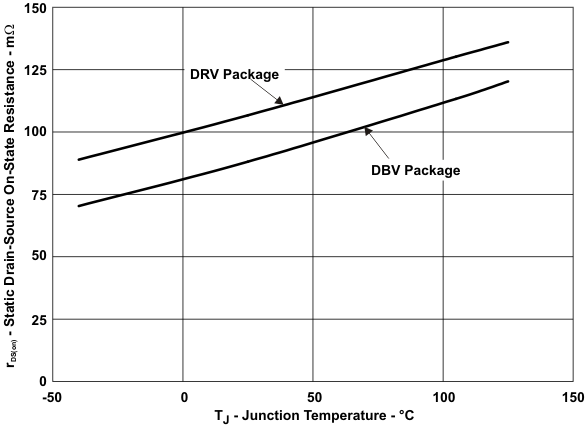
| rDS(on) | Static drain-source on-state resistance | DBV package, TJ = 25°C | 85 | 95 | mΩ | ||||
| DBV package, –40°C ≤TJ ≤125°C | 135 | ||||||||
| DRV package, TJ = 25°C | 100 | 115 | |||||||
| DRV package, –40°C ≤TJ ≤105°C | 140 | ||||||||
| DRV package, –40°C ≤TJ ≤125°C | 150 | ||||||||
| tr | Rise time, output | CL = 1 µF, RL = 100 Ω, (see Figure 20) |
VIN = 6.5 V | 1.1 | 1.5 | ms | |||
| VIN = 2.5 V | 0.7 | 1 | |||||||
| tf | Fall time, output | CL = 1 µF, RL = 100 Ω, (see Figure 20) |
VIN = 6.5 V | 0.2 | 0.5 | ||||
| VIN = 2.5 V | 0.2 | 0.5 | |||||||
| ENABLE INPUT EN OR EN | |||||||||
| Enable pin turn on/off threshold | 0.66 | 1.1 | V | ||||||
| IEN | Input current | VEN = 0 V or 6.5 V, VEN = 0 V or 6.5 V | –0.5 | 0.5 | µA | ||||
| ton | Turnon time | CL = 1 µF, RL = 100 Ω, (see Figure 20) | 3 | ms | |||||
| toff | Turnoff time | CL = 1 µF, RL = 100 Ω, (see Figure 20) | 3 | ms | |||||
| CURRENT LIMIT | |||||||||
| IOS | Current-limit threshold (Maximum DC output current IOUT delivered to load) and Short-circuit current, OUT connected to GND | RILIM = 15 kΩ, –40°C ≤TJ ≤105°C | 1610 | 1700 | 1800 | mA | |||
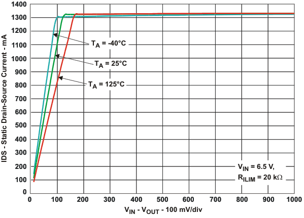
| RILIM = 20 kΩ | TJ = 25°C | 1215 | 1295 | 1375 | |||||
| –40°C ≤TJ ≤125°C | 1200 | 1295 | 1375 | ||||||
| RILIM = 49.9 kΩ | TJ = 25°C | 490 | 520 | 550 | |||||
| –40°C ≤TJ ≤125°C | 475 | 520 | 565 | ||||||
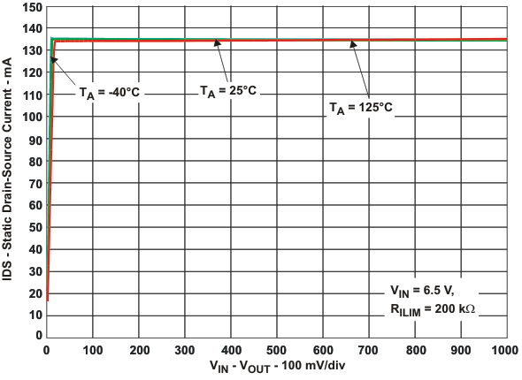
| RILIM = 210 kΩ | 110 | 130 | 150 | ||||||
| ILIM shorted to IN | 50 | 75 | 100 | ||||||
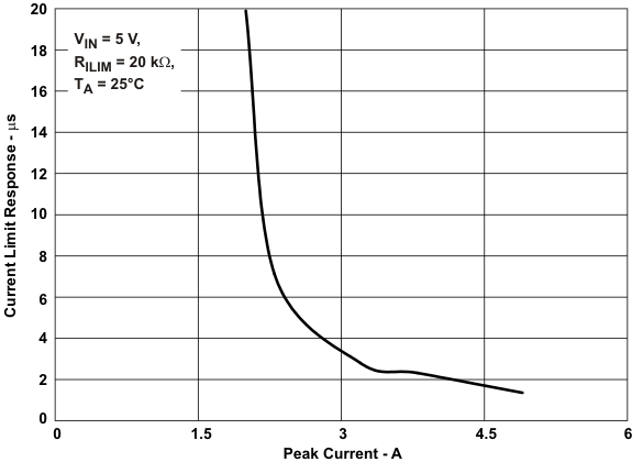
| tIOS | Response time to short circuit | VIN = 5 V (see Figure 21) | 2 | µs | |||||
| REVERSE-VOLTAGE PROTECTION | |||||||||
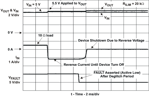
| Reverse-voltage comparator trip point (VOUT – VIN) |
95 | 135 | 190 | mV | |||||
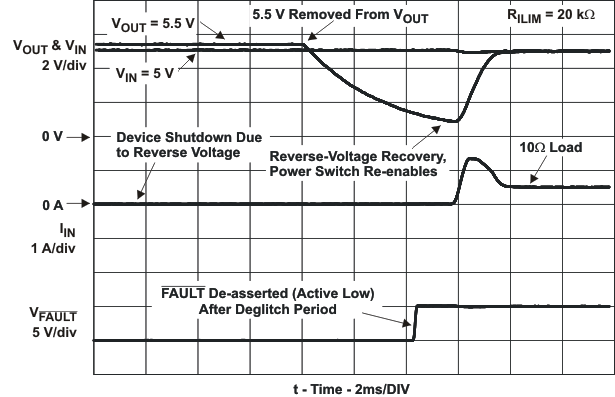
| Time from reverse-voltage condition to MOSFET turn off | VIN = 5 V | 3 | 5 | 7 | ms | ||||
| SUPPLY CURRENT | |||||||||
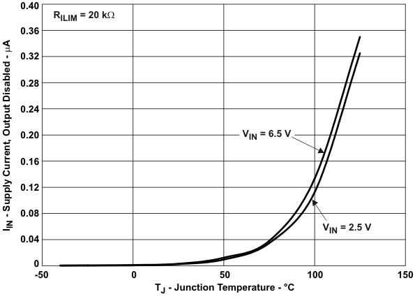
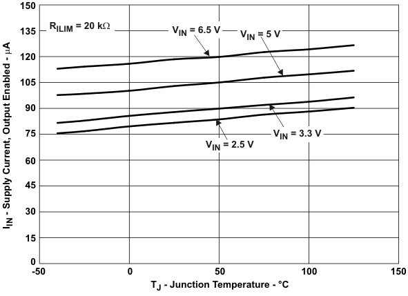
| IIN_off | Supply current, low-level output | VIN = 6.5 V, No load on OUT, VEN = 6.5 V or VEN = 0 V | 0.1 | 1 | µA | ||||
| IIN_on | Supply current, high-level output | VIN = 6.5 V, No load on OUT | RILIM = 20 kΩ | 120 | 140 | µA | |||
| RILIM = 210 kΩ | 100 | 120 | µA | ||||||
| IREV | Reverse leakage current | VOUT = 6.5 V, VIN = 0 V | TJ = 25 °C | 0.01 | 1 | µA | |||
| UNDERVOLTAGE LOCKOUT | |||||||||
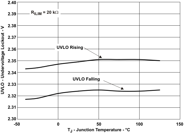
| UVLO | Low-level input voltage, IN | VIN rising | 2.35 | 2.45 | V | ||||
| Hysteresis, IN | TJ = 25 °C | 25 | mV | ||||||
| FAULT FLAG | |||||||||
| VOL | Output low voltage, FAULT | I/FAULT = 1 mA | 180 | mV | |||||
| Off-state leakage | V/FAULT = 6.5 V | 1 | µA | ||||||
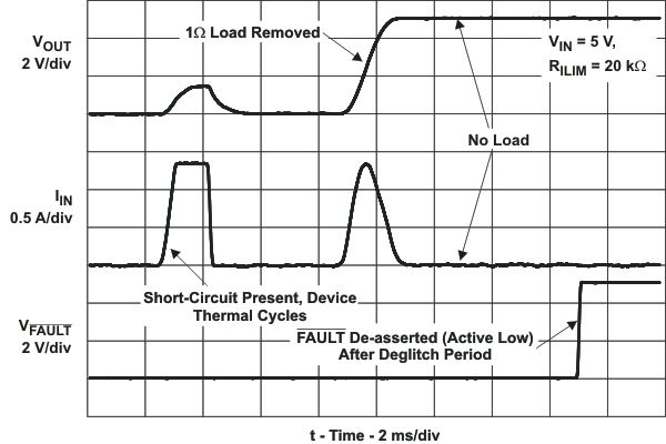
| FAULT deglitch | FAULT assertion or de-assertion due to overcurrent condition | 5 | 7.5 | 10 | ms | ||||
| FAULT assertion or de-assertion due to reverse-voltage condition | 2 | 4 | 6 | ms | |||||
| THERMAL SHUTDOWN | |||||||||
| Thermal shutdown threshold | 155 | °C | |||||||
| Thermal shutdown threshold in current-limit | 135 | °C | |||||||
| Hysteresis | 10 | °C | |||||||
(1) Pulse-testing techniques maintain junction temperature close to ambient temperature; thermal effects must be taken into account separately.
7.6 Typical Characteristics
