JAJSCO2 November 2016 TPS25810-Q1
PRODUCTION DATA.
- 1 特長
- 2 アプリケーション
- 3 概要
- 4 改訂履歴
- 5 Pin Configuration and Functions
- 6 Specifications
-
7 Detailed Description
- 7.1 Overview
- 7.2 Functional Block Diagram
- 7.3
Feature Description
- 7.3.1 Configuration Channel Pins CC1 and CC2
- 7.3.2 Current Capability Advertisement and Overload Protection
- 7.3.3
Undervoltage Lockout (UVLO)
- 7.3.3.1 Device Power Pins (IN1, IN2, AUX, OUT, and GND)
- 7.3.3.2 FAULT Response
- 7.3.3.3 Thermal Shutdown
- 7.3.3.4 REF
- 7.3.3.5 Audio Accessory Detection
- 7.3.3.6 Debug Accessory Detection
- 7.3.3.7 Plug Polarity Detection
- 7.3.3.8 Device Enable Control
- 7.3.3.9 Load Detect
- 7.3.3.10 Power Wake
- 7.3.3.11 Port Power Management (PPM)
- 7.3.3.12 Implementing PPM in a System With Two Type-C Ports
- 7.3.3.13 PPM Operation
- 7.4 Device Functional Modes
- 8 Application and Implementation
- 9 Power Supply Recommendations
- 10Layout
- 11デバイスおよびドキュメントのサポート
- 12メカニカル、パッケージ、および注文情報
7 Detailed Description
7.1 Overview
The TPS25810-Q1 device is a highly integrated USB Type-C™ downstream-facing port (DFP) controller with built-in power switch developed for the new USB Type-C connector and cable. The device provides all of the functionality needed to support a USB Type-C DFP in a system where USB power delivery (PD) source capabilities (for example, VBUS > 5 V) are not implemented. The device is designed to be compliant with the Type‑C specification, revision 1.1.
7.1.1 USB Type-C Basic
For a detailed description of the Type-C specification, see the USB-IF Web site to download the latest released version. Some of the basic concepts of the Type-C specification that pertain to understanding the operation of the TPS25810-Q1 device (a DFP device) are described as follows.
USB Type-C removes the need for different plug and receptacle types for host and device functionality. The Type-C receptacle replaces both Type-A and Type-B receptacles because the Type-C cable is pluggable in either direction between host and device. A host-to-device logical relationship is maintained via the configuration channel (CC). Optionally, hosts and devices can be either providers or consumers of power when USB PD communication is used to swap roles.
All USB Type-C ports operate in one of the following three data modes:
- Host mode: the port can only be host (provider of power).
- Device mode: the port can only be device (consumer of power).
- Dual-role mode: the port can be either host or device.
Port types:
- DFP (downstream facing port): Host
- UFP (upstream facing port): Device
- DRP (dual-role port): Host or device
Valid DFP-to-UFP connections:
- Table 1 describes valid DFP-to-UFP connections.
- Host-to-host and device-to-device have no functions.
Table 1. DFP-to-UFP Connections
| HOST-MODE PORT | DEVICE-MODE PORT | DUAL-ROLE PORT | |
|---|---|---|---|
| Host-mode port | No function | Works | Works |
| Device-mode port | Works | No function | Works |
| Dual-role port | Works | Works | Works(1) |
7.1.2 Configuration Channel
The function of the configuration channel (CC) is to detect connections and configure the interface across the USB Type-C cables and connectors.
Functionally, the configuration channel serves the following purposes:
- Detect connection to the USB ports
- Resolve cable orientation and twist connections to establish USB data bus routing
- Establish DFP and UFP roles between two connected ports
- Discover and configure power: USB Type-C current modes or USB power delivery
- Discover and configure optional alternate and accessory modes
- Enhance flexibility and ease of use
Typical flow of DFP to UFP configuration is shown in Figure 11:
 Figure 11. Flow of DFP to UFP Configuration
7.1.3 Detecting a Connection
DFPs and DRPs fulfill the role of detecting a valid connection over USB Type-C. Figure 12 shows a DFP-to-UFP connection made with Type-C cable. As shown in Figure 12, the detection concept is based on being able to detect terminations in the product that has been attached. A pullup and pulldown termination model is used. A pullup termination can be replaced by a current source.
- In the DFP-UFP connection, the DFP monitors both CC pins for a voltage lower than the unterminated voltage.
- A UFP advertises Rd on both its CC pins (CC1 and CC2).
- A powered cable advertises Ra on only one of the CC pins of the plug. Ra is used to inform the source to apply VCONN.
- An analog audio device advertises Ra on both CC pins of the plug, which identifies it as an analog audio device. VCONN is not applied on either CC pin in this case.
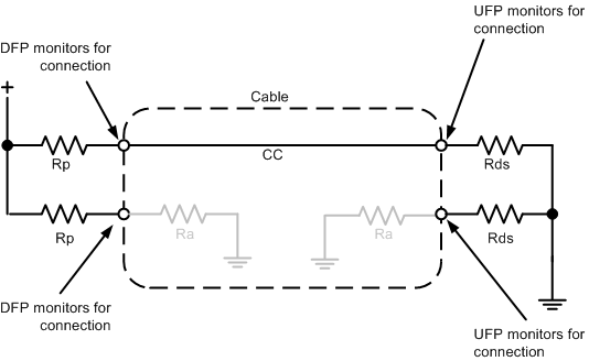 Figure 12. DFP-UFP Connection
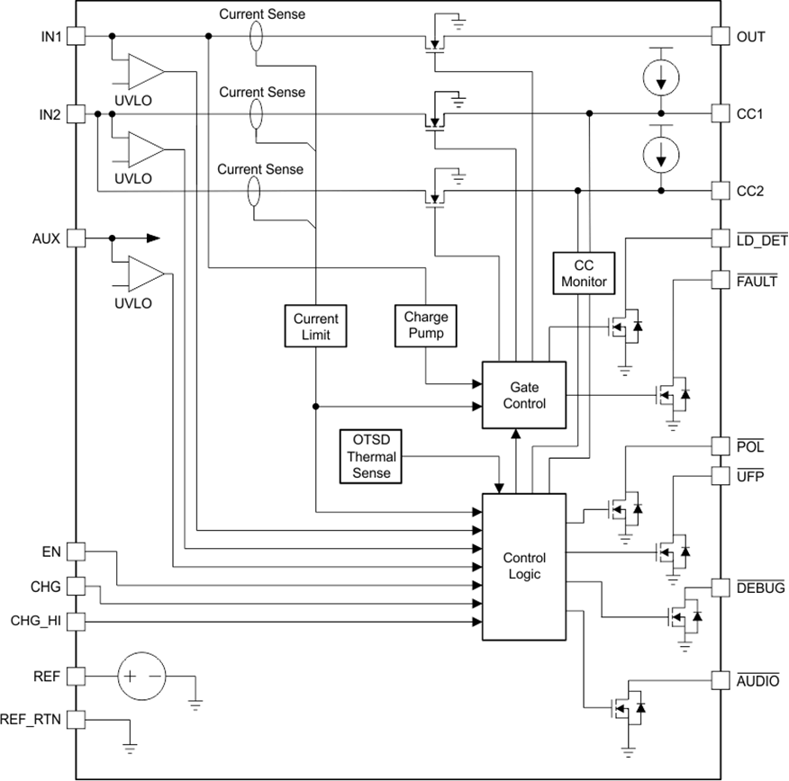
7.2 Functional Block Diagram
7.3 Feature Description
The TPS25810-Q1 device is a DFP Type-C port controller with integrated power switches for VCONN and VBUS. The TPS25810-Q1 device does not support BC1.2 charging modes, because it does not interact with USB D+ and D– data lines. The TPS25810-Q1 device can be used in conjunction with a BC 1.2 device like the TPS2514A-Q1 to support BC1.2 and Type-C charging modes in a single Type-C DFP port. See the TPS25810 EVM user's guide (SLVUAI0) and Application and Implementation section of this data sheet for more details. The TPS25810-Q1 device can be used in a USB 2.0 only or in a USB 3.1 port implementation. When used in a USB 3.1 port, the TPS25810-Q1 device can control an external super-speed MUX to handle the Type-C flippable feature.
7.3.1 Configuration Channel Pins CC1 and CC2
The TPS25810-Q1 device has two pins, CC1 and CC2, that serve to detect an attachment to the port and to resolve cable orientation. These pins are also used to establish the current broadcast to a valid UFP, configure VCONN, and detect attachment of a debug or audio-adapter accessory.
Table 2 lists the TPS25810-Q1 response to various attachments to its port.
Table 2. TPS25810-Q1 Response
| TPS25810-Q1 TYPE-C PORT | CC1 | CC2 | TPS25810-Q1 RESPONSE(1) | |||||
|---|---|---|---|---|---|---|---|---|
| OUT | VCONN
on CC1 or CC2 |
POL | UFP | AUDIO | DEBUG | |||
| Nothing attached | OPEN | OPEN | OPEN | NO | Hi-Z | Hi-Z | Hi-Z | Hi-Z |
| UFP connected | Rd | OPEN | IN1 | NO | Hi-Z | LOW | Hi-Z | Hi-Z |
| UFP connected | OPEN | Rd | IN1 | NO | LOW | LOW | Hi-Z | Hi-Z |
| Powered cable, no UFP connected | OPEN | Ra | OPEN | NO | Hi-Z | Hi-Z | Hi-Z | Hi-Z |
| Powered cable, no UFP connected | Ra | OPEN | OPEN | NO | Hi-Z | Hi-Z | Hi-Z | Hi-Z |
| Powered cable, UFP connected | Rd | Ra | IN1 | CC2 | Hi-Z | LOW | Hi-Z | Hi-Z |
| Powered cable, UFP connected | Ra | Rd | IN1 | CC1 | LOW | LOW | Hi-Z | Hi-Z |
| Debug accessory connected | Rd | Rd | OPEN | NO | Hi-Z | Hi-Z | Hi-Z | LOW |
| Audio-adapter accessory connected | Ra | Ra | OPEN | NO | Hi-Z | Hi-Z | LOW | Hi-Z |
7.3.2 Current Capability Advertisement and Overload Protection
The TPS25810-Q1 device supports all three Type-C current advertisements as defined by the USB Type-C standard. Current broadcast to a connected UFP is controlled by the CHG and CHG_HI pins. For each broadcast level, the device protects itself from a UFP that draws current in excess of the USB Type-C current advertisement of that port by setting the current limit as shown in Table 3.
Table 3. USB Type-C Current Advertisement
| CHG | CHG_HI | CC CAPABILITY BROADCAST | CURRENT LIMIT (TYP) | LOAD DETECT THRESHOLD (TYP) |
|---|---|---|---|---|
| 0 | 0 | STD | 1.7 A | NA |
| 0 | 1 | STD | 1.7 A | NA |
| 1 | 0 | 1.5 A | 1.7 A | NA |
| 1 | 1 | 3 A | 3.4 A | 1.95 A |
Under OUT overload conditions, an internal OUT current-limit regulator limits the output current to the selected ILIM based on CHG and CHG_HI selection. In applications where VCONN is supplied via CC1 or CC2, separate fixed current-limit regulators protect these pins from overload at the level indicated in the Electrical Characteristics table. When an overload condition is present, the device maintains a constant output current, with the output voltage determined by (IOS × RLOAD). Two possible overload conditions can occur. The first overload condition occurs when either: 1) input voltage is first applied, enable is true, and a short circuit is present (load which draws IOUT > IOS), or 2) input voltage is present and the TPS25810-Q1 device is enabled into a short circuit. The output voltage is held near zero potential with respect to ground and the TPS25810-Q1 device ramps the output current to IOS. The TPS25810-Q1 device limits the current to IOS until the overload condition is removed or the device begins to thermal cycle. This is demonstrated in Figure 24 where the device was enabled into a short, and subsequently cycles current off and on as the thermal protection engages.
The second condition is when an overload occurs while the device is enabled and fully turned on. The device responds to the overload condition within time tios (see Figure 1) when the specified overload (per Electrical Characteristics) is applied. The response speed and shape vary with the overload level, input circuit, and rate of application. The current-limit response varies between simply settling to IOS or turnoff and controlled return to IOS. Similar to the previous case, the TPS25810-Q1 device limits the current to IOS until the overload condition is removed or the device begins to thermal cycle.
The TPS25810-Q1 device thermal cycles if an overload condition is present long enough to activate thermal limiting in any of the above cases. This is due to the relatively large power dissipation [(VIN – VOUT) × IOS] driving the junction temperature up. The device turns off when the junction temperature exceeds 135°C (min) while in current limit. The device remains off until the junction temperature cools 20°C and then restarts. The TPS25810‑Q1 current-limit profile is shown in Figure 13.
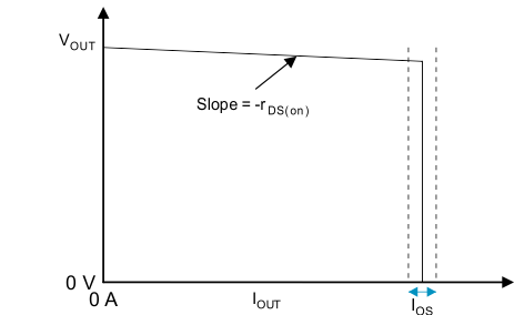 Figure 13. Current Limit Profile
7.3.3 Undervoltage Lockout (UVLO)
The undervoltage lockout (UVLO) circuit disables the power switch until the input voltage reaches the UVLO turnon threshold. Built-in hysteresis prevents unwanted on-off cycling due to input voltage droop during turnon.
7.3.3.1 Device Power Pins (IN1, IN2, AUX, OUT, and GND)
The device has multiple input power pins: IN1, IN2 and AUX. IN1 is connected to OUT by the internal power FET and serves the supply for the Type-C charging current. IN2 is the supply for VCONN and ties directly between the VCONN power switch on its input and CC1 or CC2 on its output. AUX, the auxiliary input supply, provides power to the device. See the Functional Block Diagram.
In the simplest implementation where multiple supplies are not available; IN1, IN2, and AUX can be tied together. However, in mobile systems (battery powered) where system power savings is paramount, IN1 and IN2 can be powered by the high-power dc-dc supply (>3-A capability), and AUX can be connected to the low-power supply that typically powers the system microcontroller when the system is in the hibernate or sleep power state. Unlike IN1 and IN2, AUX can operate directly from a 3.3-V supply commonly used to power the microcontroller when the system is put in low-power mode. Ceramic bypass capacitors close to the device from the INx and AUX pins to GND are recommended to alleviate bus transients.
The recommended operating voltage range for IN1 and IN2 is 4.5 V to 5.5 V, whereas AUX can be operated from 2.9 V to 5.5 V. However IN1, the high-power supply, can operate up to 6.5 V. This higher input voltage affords a larger IR loss budget in systems where a long cable harness is used, and results in high IR losses with 3-A charging current. Increasing IN1 beyond 5.5 V enables longer cable and board trace lengths between the device and the Type-C receptacle while meeting the USB specification for VBUS ≥ 4.75 V at the connector.
Figure 14 illustrates the point. In this example IN1 is at 5 V, which restricts the IR loss budget from the dc-dc converter to the connector to 250 mV.
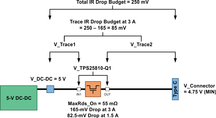 Figure 14. Total IR Loss Budget
7.3.3.2 FAULT Response
The FAULT pin is an open-drain output asserted low when the device OUT current exceeds its programmed value and the overtemperature threshold (TTH_OTSD1) is crossed. See the Electrical Characteristics for overcurrent and overtemperature values. The FAULT signal remains asserted until the fault condition is removed and the device resumes normal operation. The TPS25810-Q1 device is designed to eliminate false overcurrent fault reporting by using an internal deglitch circuit.
Connect FAULT with a pullup resistor to AUX. FAULT can be left open or tied to GND when not used.
7.3.3.3 Thermal Shutdown
The device has two internal overtemperature shutdown thresholds, TTH_OTSD1 and TTH_OTSD2, to protect the internal FET from damage and assist with overall safety of the system. TTH_OTSD2 is greater than TTH_OTSD1. FAULT is asserted low to signal a fault condition when the device temperature exceeds TTH_OTSD1 and the current-limit switch is disabled. However when TTH_OTSD2 is exceeded, all open-drain outputs are left open and the device is disabled such that minimum power and heat are dissipated. The device attempts to power up when the die temperature decreases by 20°C.
7.3.3.4 REF
A 100-kΩ (1% or better recommended) resistor is connected from this pin to REF_RTN. The REF pin sets the reference current required to bias the internal circuitry of the device. The overload current-limit tolerance and CC currents depend upon the accuracy of this resistor. Using a ±1% or better low-temperature-coefficient resistor yields the best current-limit accuracy and overall device performance.
7.3.3.5 Audio Accessory Detection
The USB Type-C specification defines an audio-adapter decode state which allows implementation of an analog USB Type-C to 3.5-mm headset adapter. The TPS25810-Q1 device detects an audio accessory device when both CC1 and CC2 pins detect VRa voltage (when pulled to ground by an Ra resistor). The device asserts the open-drain AUDIO pin low to indicate the detection of such a device.
Table 4. Audio Accessory Detection
| CC1 | CC2 | AUDIO | STATE |
|---|---|---|---|
| Ra | Ra | Asserted (pulled low) | Audio-adapter accessory connected |
Platforms supporting the audio accessory function can be triggered by the AUDIO pin to enable accessory mode circuits to support the audio function. When the Ra pulldown is removed from the CC2 pin, AUDIO is deasserted or pulled high. The TPS25810-Q1 device monitors the CC2 pin for audio device detach. When this function is not needed (for example in a data-less port), AUDIO can be tied to GND or left open.
7.3.3.6 Debug Accessory Detection
The Type-C spec supports an optional debug-accessory mode, used for debug only and not to be used for communicating with commercial products. When the TPS25810-Q1 device detects VRd voltage on both CC1 and CC2 pins (when pulled to ground by an Rd resistor), it asserts DEBUG low. With DEBUG asserted, the system can enter debug mode for factory testing or a similar functional mode. DEBUG deasserts or pulls high when Rd is removed from CC1. The TPS25810-Q1 device monitors the CC1 pin for debug-accessory detach.
If the debug-accessory mode is not used, tie DEBUG to GND or leave it open.
Table 5. Debug Accessory Detection
| CC1 | CC2 | POL | STATE |
|---|---|---|---|
| Rd | Rd | Asserted (pulled low) | Debug accessory connected |
7.3.3.7 Plug Polarity Detection
Reversible Type-C plug orientation is reported by the POL pin when a UFP is connected. However, when no UFP is attached POL remains deasserted, irrespective of cable plug orientation. Table 6 describes the POL state based on which of the device CC pins detects VRd from an attached UFP pulldown.
Table 6. Plug Polarity Detection
| CC1 | CC2 | POL | STATE |
|---|---|---|---|
| Rd | Open | Hi-Z | UFP connected |
| Open | Rd | Asserted (pulled low) | UFP connected with reverse plug orientation |
Figure 15 shows an example implementation which uses the POL terminal to control the SEL terminal on the HD3SS3212 device. The HD3SS3212 device provides switching on the differential channels between Port B and Port C to Port A, depending on cable orientation. For details on the HD3SS3212 device, see the HD3SS3212 data sheet (SLASE74).
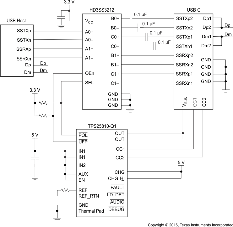 Figure 15. Example Implementation
7.3.3.8 Device Enable Control
The logic enable pin (EN) controls the power switch and device supply current. The supply current is reduced to less than 1 μA when a logic low is present on EN. The EN pin provides a convenient way to turn on or turn off the device while it is powered. The enable input threshold has built-in hysteresis. When this pin is pulled high, the device is turned on or enabled. When the device is disabled (EN pulled low) the internal FETs tied to IN1 and IN2 are disconnected, all open-drain outputs are left open (Hi-Z), and the monitor block for CC1 and CC2 is turned off. The EN terminal should not be left floating.
7.3.3.9 Load Detect
The load-detect function in the device is enabled when the device is set to broadcast high-current VBUS charging (CHG = CHG_HI = High) on the CC pin. In this mode, the device monitors the OUT current to a UFP; if the current exceeds 1.95 A (typ), the LD_DET pin asserts. Because LD_DET is an open-drain output, pull it high with 100 kΩ to AUX when used; tie it to GND or leave it open when not used.
7.3.3.10 Power Wake
The power-wake feature supported in the TPS25810-Q1 device offers the mobile-systems designer a way to save on system power when no UFP is attached to the Type-C port. See Figure 16. To enable power wake, the UFP pins from device No. 1 and No. 2 are tied together (each with its own 100-kΩ pullup) to the enable pin of a 5-V, 6-A dc-dc buck converter. When no UFP is detected on both Type-C ports, the EN pin of the dc-dc converter is pulled high, thereby disabling it. Because both TPS25810-Q1 devices are powered by an always-on 3.3-V LDO, turning off the supply to IN1 and IN2 does not affect its operation in detach state. Anytime a UFP is detected on either port, the corresponding TPS25810-Q1 UFP pin is pulled low, enabling the dc-dc converter to provide charging current to the attached UFP. Turning off the high-power dc-dc converter when ports are unattached saves on system power. This method can save a significant amount of power, because the TPS25810-Q1 device only requires < 5 µA when no UFP device is connected.
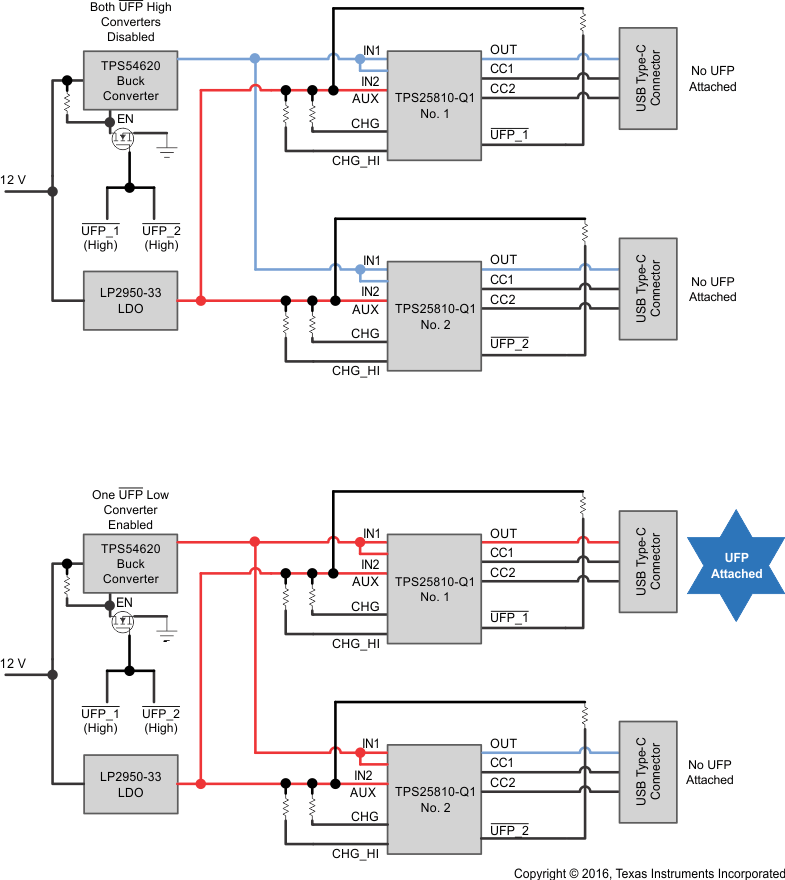 Figure 16. Power-Wake Implementation
7.3.3.11 Port Power Management (PPM)
PPM is the intelligent and dynamic allocation of power made possible with the use of the LD_DET pin. PPM is for systems that have multiple charging ports but cannot power them all at their maximum charging current simultaneously.
Goals of PPM are:
- Enhanced user experience, because the user needs not to search for a high-current charging port.
- Lowered cost and size of the power supply needed for implementing high-current charging in a multiport system.
7.3.3.12 Implementing PPM in a System With Two Type-C Ports
Figure 17 shows PPM and power wake implemented in a system with two Type-C ports, both initially set to broadcast high-current charging (3 A, CHG and CHG_HI pulled high via 100-kΩ resistors to AUX). To enable PPM, tie the LD_DET pin from TPS25810-Q1 device No. 1 to CHG_HI of TPS25810-Q1 device No. 2 and vice versa, as shown in Figure 17. Each device independently monitors the charging current drawn by its attached UFP.
IN1 and IN2 are connected to a TPS54620, a 6-A synchronous step-down converter. AUX is powered by an LP2950-33, a low-quiescent-current 3.3-V LDO. With no UFP attached to either Type-C port, the TPS25810-Q1 device is powered by the LP2950-33. This method saves a significant amount of power, because the TPS25810‑Q1 device requires less than 2 µA when no USB device is connected.
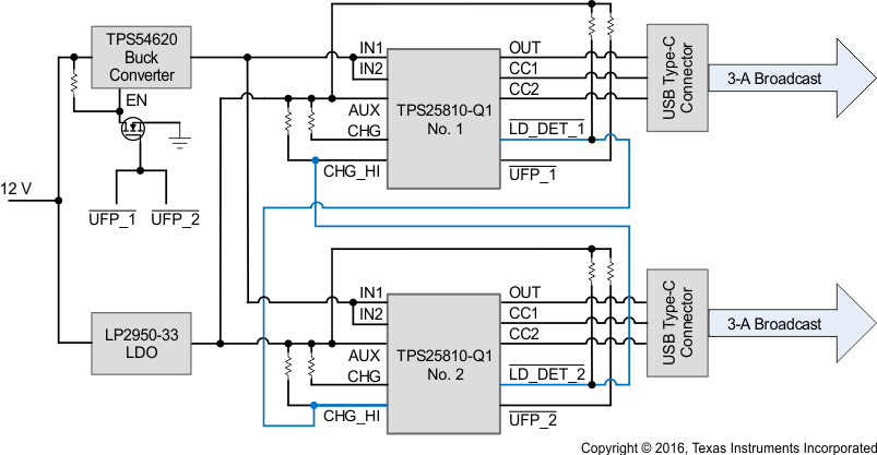 Figure 17. PPM and Power Wake Implemented
7.3.3.13 PPM Operation
When no UFP is attached, or either of the two attached UFPs is drawing current less than the LD_DET threshold (1.95 A typical), the LD_DET output for both devices is high (shown in blue in Figure 18). Now when a UFP is attached to device No. 1 that draws a charging current higher than the LD_DET threshold (1.95 A), this causes LD_DET to assert or pull low (shown in red in Figure 18). Because the LD-DET pins of the No. 1 and No. 2 devices are connected to the CHG_HI pins of each other, a high-current detection on device No. 1 forces device No. 2 to broadcast 1.5 A or medium charging-current capability on its CC pin. The Type-C specification requires a UFP to monitor the CC pins continuously and adjust its current consumption (within 60 ms) to remain within the value advertised by the DFP.
Figure 19 shows the case when a UFP attached to device No. 1 reduces its charging current below the LD_DET threshold, which causes LD-DET to de-assert, thereby toggling the device No. 2 CH_HI pin from low to high.
This scheme:
- Delivers a better user experience, as the user has no worry about the maximum charging current rating of the host ports. Both ports initially advertise high-current charging.
- Enables a smaller and lower-cost power supply, as the loading is controlled and never allowed to exceed 5 A.
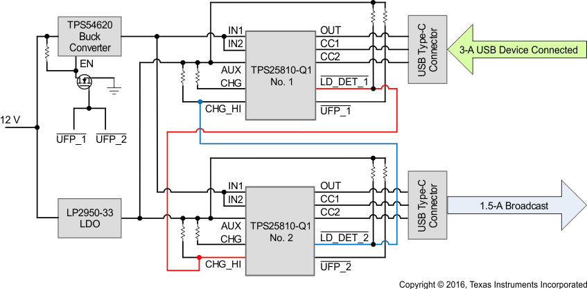 Figure 18. 3-A USB Device Connected
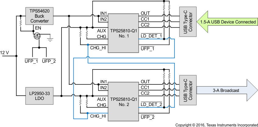 Figure 19. 1.5-A USB Device Connected
7.4 Device Functional Modes
The TPS25810-Q1 device is a Type-C controller with integrated power switch that supports all Type-C functions in a downstream facing port. The device is also used to manage current advertisement and protection for a connected UFP and active cable. The device starts its operation by monitoring the AUX bus. When VAUX exceeds the undervoltage-lockout threshold, the device samples the EN pin. A high level on this pin enables the device, and normal operation begins. Having successfully completed its start-up sequence, the device now actively monitors its CC1 and CC2 pins for attachment to a UFP. When a UFP is detected on either the CC1 or CC2 pin, the internal MOSFET starts to turn on after the required debounce time is met. The internal MOSFET starts conducting and allows current to flow from IN1 to OUT. If Ra is detected on the other CC pin (not connected to the UFP), VCONN is applied to allow current to flow from IN2 to the CC pin connected to Ra. For a complete listing of various device operational modes, see Table 2.