JAJSLC2C march   2014  – march 2021 TPS3700-Q1

PRODUCTION DATA  

  1.   1
  2. 特長
  3. アプリケーション
  4. 概要
  5. Revision History
  6. Pin Configuration and Functions
  7. Specifications
    1. 6.1 Absolute Maximum Ratings
    2. 6.2 ESD Ratings
    3. 6.3 Recommended Operating Conditions
    4. 6.4 Thermal Information
    5. 6.5 Electrical Characteristics
    6. 6.6 Timing Requirements
    7. 6.7 Timing Diagram
    8. 6.8 Switching Characteristics
    9. 6.9 Typical Characteristics
  8. Detailed Description
    1. 7.1 Overview
    2. 7.2 Functional Block Diagram
    3. 7.3 Feature Description
      1. 7.3.1 Inputs (INA+, INB–)
      2. 7.3.2 Outputs (OUTA, OUTB)
      3. 7.3.3 Window Voltage Detector
      4. 7.3.4 Immunity to Input Terminal Voltage Transients
    4. 7.4 Device Functional Modes
  9. Application and Implementation
    1. 8.1 Application Information
      1. 8.1.1 VPULLUP to a Voltage Other Than VDD
      2. 8.1.2 Monitoring VDD
      3. 8.1.3 Monitoring a Voltage Other Than VDD
      4. 8.1.4 Monitoring Overvoltage and Undervoltage for Separate Rails
    2. 8.2 Typical Application
      1. 8.2.1 Design Requirements
        1. 8.2.1.1 Input Supply Capacitor
        2. 8.2.1.2 Input Capacitors
      2. 8.2.2 Detailed Design Procedure
      3. 8.2.3 Application Curves
  10. Power Supply Recommendations
  11. 10Layout
    1. 10.1 Layout Guidelines
    2. 10.2 Layout Example
  12. 11Device and Documentation Support
    1. 11.1 Documentation Support
      1. 11.1.1 Related Documentation
    2. 11.2 Trademarks
    3. 11.3 静電気放電に関する注意事項
    4. 11.4 用語集
  13. 12Mechanical, Packaging, and Orderable Information

パッケージ・オプション

メカニカル・データ(パッケージ|ピン)
サーマルパッド・メカニカル・データ
発注情報

Monitoring Overvoltage and Undervoltage for Separate Rails

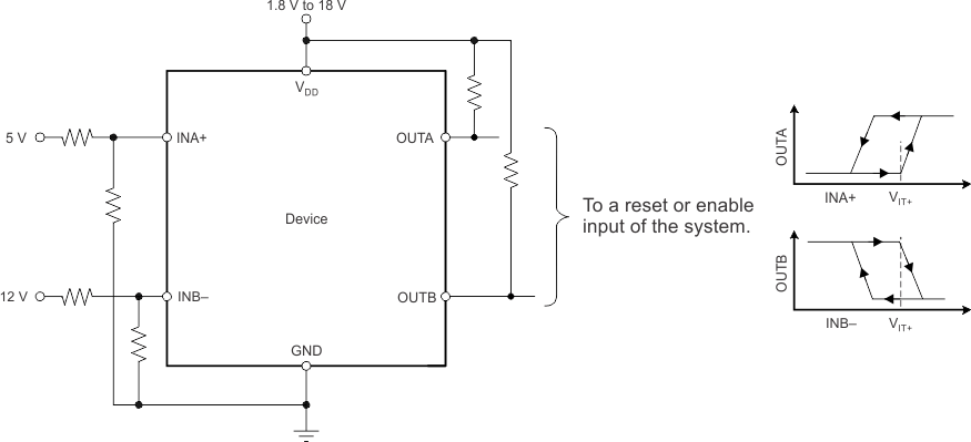
Some applications may want to monitor for overvoltage conditions on one rail while also monitoring for undervoltage conditions on a different rail. In those applications two independent resistor dividers will need to be used.
GUID-BE05AEDA-5398-41CD-8959-862665B4A348-low.gif
NOTE: In this case, OUTA is driven low when an undervoltage condition is detected at the 5-V rail and OUTB is driven low when an overvoltage condition is detected at the 12-V rail.
Figure 8-4 Monitoring Overvoltage for One Rail and Undervoltage for a Different Rail