JAJSGL5C December 2018 – August 2019 TPS3840
PRODUCTION DATA.
- 1 特長
- 2 アプリケーション
- 3 概要
- 4 改訂履歴
- 5 概要 (続き)
- 6 Device Comparison Table
- 7 Pin Configuration and Functions
- 8 Specifications
- 9 Detailed Description
-
10Application and Implementation
- 10.1 Application Information
- 10.2 Typical Application
- 11Power Supply Recommendations
- 12Layout
- 13デバイスおよびドキュメントのサポート
- 14メカニカル、パッケージ、および注文情報
10.2.3 Design 3: Fast Start Undervoltage Supervisor with Level-shifted Input
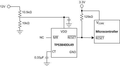
A typical application for the TPS3840 is a fast startup undervoltage supervisor that operates with an input power supply higher than the recommended maximum of 10 V through the use of a resistor divider at the input as shown in Figure 51. The TPS3840 can be used to monitor any rail above 1.6 V and only requires maximum 350 µs upon startup before the device can begin monitoring a voltage. In this design application, a TPS3840 monitors a 12-V rail and triggers a reset fault condition if the voltage rail voltage drops below 10 V using a TPS3840 device with VIT- of 4.9 V. This design also accounts for a wide input range in the case the 12-V rail rises higher, the resistor divider is set so that the voltage at the VDD pin never exceeds 10 V. The resistor values must not be so large that the external resistor divider affects the accuracy or operation of the device. TPS3840 is available in both active-low and active-high topologies providing the flexibility to monitor undervoltage or overvoltage with either output logic. This design uses the active-low, open-drain TPS3840DL49 variant so that when the undervoltage condition occurs, that is when the voltage at VDD pin falls below the voltage threshold set by the external resistor divider, the output transitions to logic-low and can be used to flag an undervoltage condition or used to connect to the ENABLE of the next device to shut it off as a logic low on an ENABLE pin typically disables the device. In this design, the output of the TPS3840 simply connects to a MCU to flag an undervoltage condition.
 Figure 51. Fast Start Undervoltage Supervisor with Level-shifted Input