JAJSGL5C December   2018  – August 2019 TPS3840

PRODUCTION DATA.  

  1. 特長
  2. アプリケーション
  3. 概要
    1.     Device Images
      1.      代表的なアプリケーション回路
      2.      TPS3840 の標準的な消費電流
  4. 改訂履歴
  5. 概要 (続き)
  6. Device Comparison Table
  7. Pin Configuration and Functions
    1.     Pin Functions
  8. Specifications
    1. 8.1 Absolute Maximum Ratings
    2. 8.2 ESD Ratings
    3. 8.3 Recommended Operating Conditions
    4. 8.4 Thermal Information
    5. 8.5 Electrical Characteristics
    6. 8.6 Timing Requirements
    7. 8.7 Typical Characteristics
  9. Detailed Description
    1. 9.1 Overview
    2. 9.2 Functional Block Diagram
    3. 9.3 Feature Description
      1. 9.3.1 Input Voltage (VDD)
        1. 9.3.1.1 VDD Hysteresis
        2. 9.3.1.2 VDD Transient Immunity
      2. 9.3.2 User-Programmable Reset Time Delay
      3. 9.3.3 Manual Reset (MR) Input
      4. 9.3.4 Output Logic
        1. 9.3.4.1 RESET Output, Active-Low
        2. 9.3.4.2 RESET Output, Active-High
    4. 9.4 Device Functional Modes
      1. 9.4.1 Normal Operation (VDD > VDD(min))
      2. 9.4.2 VDD Between VPOR and VDD(min)
      3. 9.4.3 Below Power-On-Reset (VDD < VPOR)
  10. 10Application and Implementation
    1. 10.1 Application Information
    2. 10.2 Typical Application
      1. 10.2.1 Design 1: Dual Rail Monitoring with Power-Up Sequencing
        1. 10.2.1.1 Design Requirements
        2. 10.2.1.2 Detailed Design Procedure
        3. 10.2.1.3 Application Curves
      2. 10.2.2 Design 2: Battery Voltage and Temperature Monitor
        1. 10.2.2.1 Design Requirements
        2. 10.2.2.2 Detailed Design Procedure
      3. 10.2.3 Design 3: Fast Start Undervoltage Supervisor with Level-shifted Input
        1. 10.2.3.1 Design Requirements
        2. 10.2.3.2 Detailed Design Procedure
      4. 10.2.4 Design 4: Voltage Monitor with Back-up Battery Switchover
        1. 10.2.4.1 Design Requirements
        2. 10.2.4.2 Detailed Design Procedure
      5. 10.2.5 Application Curve: TPS3840EVM
  11. 11Power Supply Recommendations
  12. 12Layout
    1. 12.1 Layout Guidelines
    2. 12.2 Layout Example
  13. 13デバイスおよびドキュメントのサポート
    1. 13.1 デバイスの項目表記
    2. 13.2 コミュニティ・リソース
    3. 13.3 商標
    4. 13.4 静電気放電に関する注意事項
    5. 13.5 Glossary
  14. 14メカニカル、パッケージ、および注文情報

パッケージ・オプション

メカニカル・データ(パッケージ|ピン)
サーマルパッド・メカニカル・データ
発注情報

Design 4: Voltage Monitor with Back-up Battery Switchover

A typical application for the TPS3840 is to monitor a voltage rail and switch the power to a back-up battery if the main supply is in undervoltage condition. Because systems that utilize a back-up battery tend to require low quiescent current, TPS3840 serves as the perfect solution as this device only requires 350 nA typically. The TPS3840 monitors the main power rail via the VDD pin and when the main power rail falls, the RESET output asserts causing a switch to close on the back-up battery rail. The diodes provide an ORing logic function to prevent reverse leakage and to allow either rail to connect to the output depending on the status of the main voltage rail.
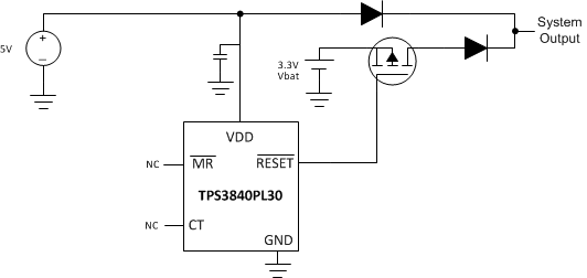
TPS3840 Typical_Application_4rev4.gifFigure 52. Voltage Monitor with Back-up Battery Switchover Solution