JAJSCT5A March 2016 – May 2016 TPS3890
PRODUCTION DATA.
- 1 特長
- 2 アプリケーション
- 3 概要
- 4 改訂履歴
- 5 Device Comparison Table
- 6 Pin Configuration and Functions
- 7 Specifications
- 8 Detailed Description
- 9 Application and Implementation
- 10Power Supply Recommendations
- 11Layout
- 12デバイスおよびドキュメントのサポート
- 13メカニカル、パッケージ、および注文情報
8 Detailed Description
8.1 Overview
The TPS3890 supervisory product family is designed to assert a RESET signal when either the SENSE pin voltage drops below VITN or the manual reset (MR) is driven low. The RESET output remains asserted for a user-adjustable time after both the manual reset (MR) and SENSE voltages return above their respective thresholds.
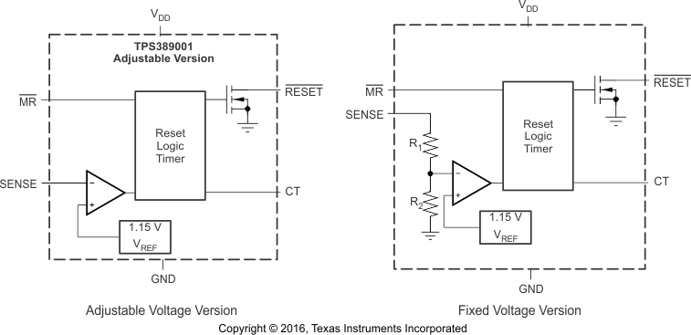
8.2 Functional Block Diagram

8.3 Feature Description
The combination of user-adjustable reset delay time with a broad range of threshold voltages allow these devices to be used in a wide array of applications. Fixed negative threshold voltages (VITN) can be factory set from 1.15 V to 3.17 V (see the Device Comparison Table for available options), and the adjustable device can be used to customize the threshold voltage for other application needs by using an external resistor divider. The CT pin allows the reset delay to be set between 25 μs and 30 s with the use of an external capacitor.
8.3.1 User-Configurable RESET Delay Time
The rising RESET delay time (tPD(r)) can be configured by installing a capacitor connected to the CT pin. The TPS3890 uses a CT pin charging current (ICT) of 1.15 µA to help counter the effect of capacitor and board-level leakage currents that can be substantial in certain applications. The rising RESET delay time can be set to any value between 25 µs (no CCT installed) and 30 s (CCT = 26 µF).
The capacitor value needed for a given delay time can be calculated using Equation 1:
The slope of Equation 1 is determined by the time that the CT charging current (ICT) takes to charge the external capacitor up to the CT comparator threshold voltage (VCT). When RESET is asserted, the capacitor is discharged through the internal CT pulldown resistor (RCT). When the RESET conditions are cleared, the internal precision current source is enabled and begins to charge the external capacitor and when the voltage on this capacitor reaches 1.22 V, RESET is deasserted. Note that in order to minimize the difference between the calculated RESET delay time and the actual RESET delay time, use a low-leakage type capacitor (such as a ceramic capacitor) and minimize parasitic board capacitance around this pin.
8.3.2 Manual Reset (MR) Input
The manual reset (MR) input allows a processor or other logic circuits to initiate a reset. A logic low on MR causes RESET to assert. After MR returns to a logic high and SENSE is above VITP, RESET is deasserted after the user-defined reset delay. If MR is not controlled externally, then MR must be connected to VDD. Note that if the logic signal driving MR is not greater than or equal to VDD, then some additional current flows into VDD and out of MR and the difference is apparent when comparing Figure 8 and Figure 9.
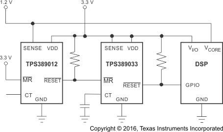
Figure 23 shows how MR can be used to monitor multiple system voltages when only a single CT capacitor is needed to set the RESET delay time.
 Figure 23. Using MR to Monitor Multiple System Voltages
8.3.3 RESET Output
RESET remains high (deasserted) as long as SENSE is above the positive threshold (VITP) and the manual reset signal (MR) is logic high. If SENSE falls below the negative threshold (VITN) or if MR is driven low, then RESET is asserted, driving the RESET pin to a low impedance.
When MR is again logic high and SENSE is above VITP, a delay circuit is enabled that holds RESET low for a specified reset delay period (tPD(r)). When the reset delay has elapsed, the RESET pin goes to a high-impedance state and uses a pullup resistor to hold RESET high. Connect the pullup resistor to the proper voltage rail to enable the outputs to be connected to other devices at the correct interface voltage level. RESET can be pulled up to any voltage up to 5.5 V, independent of the device supply voltage. To ensure proper voltage levels, give some consideration when choosing the pullup resistor values. The pullup resistor value is determined by VOL, the output capacitive loading, and the output leakage current (ILKG(OD)).
8.3.4 SENSE Input
The SENSE input can vary from ground to 5.5 V (7.0 V, absolute maximum), regardless of the device supply voltage used. The SENSE pin is used to monitor the critical voltage rail. If the voltage on this pin drops below VITN, then RESET is asserted. When the voltage on the SENSE pin exceeds the positive threshold voltage, RESET deasserts after the user-defined RESET delay time.
The internal comparator has built-in hysteresis to ensure well-defined RESET assertions and deassertions even when there are small changes on the voltage rail being monitored.
The TPS3890 device is relatively immune to short transients on the SENSE pin. Glitch immunity is dependent on threshold overdrive, as illustrated in Figure 19 for VITN and Figure 18 for VITP. Although not required in most cases, for noisy applications good analog design practice is to place a 1-nF to 10-nF bypass capacitor at the SENSE input to reduce sensitivity to transient voltages on the monitored signal.
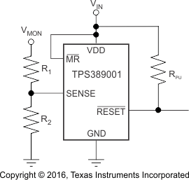
The adjustable version (TPS389001) can be used to monitor any voltage rail down to 1.15 V using the circuit shown in Figure 24.
 Figure 24. Using the TPS389001 to Monitor a User-Defined Threshold Voltage
The target threshold voltage for the monitored supply (VITx(MON)) and the resistor divider values can be calculated by using Equation 2 and Equation 3, respectively:
Equation 3 can be used to calculate either the negative threshold or the positive threshold by replacing VITx with either VITN or VITP, respectively.
Resistors with high values minimize current consumption; however, the input bias current of the device degrades accuracy if the current through the resistors is too low. Therefore, choosing an RTOTAL value so that the current through the resistor divider is at least 100 times larger than the SENSE input current is simplest. See application report Optimizing Resistor Dividers at a Comparator Input (SLVA450) for more details on sizing input resistors.
8.3.4.1 Immunity to SENSE Pin Voltage Transients
The TPS3702 is immune to short voltage transient spikes on the input pins. Sensitivity to transients depends on both transient duration and overdrive (amplitude) of the transient. Overdrive is defined by how much VSENSE exceeds the specified threshold, and is important to know because the smaller the overdrive, the slower the response of the outputs (that is, undervoltage and overvoltage). Threshold overdrive is calculated as a percent of the threshold in question, as shown in Equation 4.
Figure 17 to Figure 20 illustrate the glitch immunity that the TPS3890 has versus temperature with three different overdrive voltages. The propagation delay versus overdrive curves (Figure 13 to Figure 16) can be used to determine how sensitive the TPS3890 family of devices are across an even wider range of overdrive voltages.
8.4 Device Functional Modes
Table 1 summarizes the various functional modes of the device.
Table 1. Truth Table
| VDD | MR | SENSE | RESET |
|---|---|---|---|
| VDD < VPOR | — | — | Undefined |
| VPOR < VDD < VDD(MIN)(1) | — | — | L |
| VDD ≥ VDD(MIN) | L | — | L |
| VDD ≥ VDD(MIN) | H | VSENSE < VITN | L |
| VDD ≥ VDD(MIN) | H | VSENSE > VITP | H |
8.4.1 Normal Operation (VDD > VDD(min))
When VDD is greater than VDD(min), the RESET signal is determined by the voltage on the SENSE pin and the logic state of MR.
- MR high: when the voltage on VDD is greater than 1.5 V, the RESET signal corresponds to the voltage on the SENSE pin relative to the threshold voltage.
- MR low: in this mode, RESET is held low regardless of the voltage on the SENSE pin.
8.4.2 Above Power-On-Reset But Less Than VDD(min) (VPOR < VDD < VDD(min))
When the voltage on VDD is less than the VDD(min) voltage, and greater than the power-on-reset voltage (VPOR), the RESET signal is asserted regardless of the voltage on the SENSE pin.
8.4.3 Below Power-On-Reset (VDD < VPOR)
When the voltage on VDD is lower thanVPOR, the device does not have enough voltage to internally pull the asserted output low and RESET is undefined and must not be relied upon for proper device function.