JAJSIJ2C September   2020  – January 2024 TPS3899

PRODUCTION DATA  

  1.   1
  2. 特長
  3. アプリケーション
  4. 概要
  5. Device Comparison
  6.   Pin Configuration and Functions
  7. Specifications
    1. 5.1 Absolute Maximum Ratings
    2. 5.2 ESD Ratings
    3. 5.3 Recommended Operating Conditions
    4. 5.4 Thermal Information
    5. 5.5 Electrical Characteristics
    6. 5.6 Timing Requirements
    7. 5.7 Timing Diagrams
    8. 5.8 Typical Characteristics
  8. Detailed Description
    1. 6.1 Overview
    2. 6.2 Functional Block Diagram
    3. 6.3 Feature Description
      1. 6.3.1 VDD Hysteresis
      2. 6.3.2 User-Programmable Sense and Reset Time Delay
      3. 6.3.3 RESET/RESET Output
      4. 6.3.4 SENSE Input
        1. 6.3.4.1 Immunity to SENSE Pin Voltage Transients
    4. 6.4 Device Functional Modes
      1. 6.4.1 Normal Operation (VDD > VDD(min))
      2. 6.4.2 Above Power-On-Reset But Less Than VDD(min) (VPOR < VDD < VDD(min))
      3. 6.4.3 Below Power-On-Reset (VDD < VPOR)
  9. Application and Implementation
    1. 7.1 Application Information
    2. 7.2 Typical Application
      1. 7.2.1 Design Requirements
      2. 7.2.2 Detailed Design Procedure
      3. 7.2.3 Application Curves
      4. 7.2.4 Power Supply Recommendations
      5. 7.2.5 Layout
        1. 7.2.5.1 Layout Guidelines
        2. 7.2.5.2 Layout Example
  10. Device and Documentation Support
    1. 8.1 Device Support
      1. 8.1.1 Device Nomenclature
    2. 8.2 Receiving Notification of Documentation Updates
    3. 8.3 サポート・リソース
    4. 8.4 Trademarks
    5. 8.5 静電気放電に関する注意事項
    6. 8.6 用語集
  11. Revision History
  12. 10Mechanical, Packaging, and Orderable Information

パッケージ・オプション

メカニカル・データ(パッケージ|ピン)
サーマルパッド・メカニカル・データ
発注情報

VDD Hysteresis

The internal comparator has built-in hysteresis to avoid erroneous output reset release. If the voltage at the VDD pin falls below VIT- the output reset is asserted. When the voltage at the VDD pin goes above VIT- plus hysteresis (VHYS) the output reset is deasserted after tD delay.
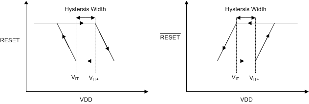
GUID-C2357FFE-5DF9-41B3-8B2B-8CABEB01FF90-low.gif Figure 6-1 Hysteresis Diagram