SLUS772G March 2008 – June 2020 TPS40210 , TPS40211
PRODUCTION DATA
- 1 Features
- 2 Applications
- 3 Description
- 4 Revision History
- 5 Pin Configuration and Functions
- 6 Specifications
-
7 Detailed Description
- 7.1 Overview
- 7.2 Functional Block Diagram
- 7.3
Feature Description
- 7.3.1 Soft Start
- 7.3.2 BP Regulator
- 7.3.3 Shutdown (DIS/ EN Pin)
- 7.3.4 Minimum On-Time and Off-Time Considerations
- 7.3.5 Setting the Oscillator Frequency
- 7.3.6 Synchronizing the Oscillator
- 7.3.7 Current Sense and Overcurrent
- 7.3.8 Current Sense and Subharmonic Instability
- 7.3.9 Current Sense Filtering
- 7.3.10 Control Loop Considerations
- 7.3.11 Gate Drive Circuit
- 7.3.12 TPS40211
- 7.4 Device Functional Modes
-
8 Application and Implementation
- 8.1 Application Information
- 8.2
Typical Applications
- 8.2.1
12-V to 24-V Nonsynchronous Boost Regulator
- 8.2.1.1 Design Requirements
- 8.2.1.2
Detailed Design Procedure
- 8.2.1.2.1 Custom Design with WEBENCH Tools
- 8.2.1.2.2 Duty Cycle Estimation
- 8.2.1.2.3 Inductor Selection
- 8.2.1.2.4 Rectifier Diode Selection
- 8.2.1.2.5 Output Capacitor Selection
- 8.2.1.2.6 Input Capacitor Selection
- 8.2.1.2.7 Current Sense and Current Limit
- 8.2.1.2.8 Current Sense Filter
- 8.2.1.2.9 Switching MOSFET Selection
- 8.2.1.2.10 Feedback Divider Resistors
- 8.2.1.2.11 Error Amplifier Compensation
- 8.2.1.2.12 RC Oscillator
- 8.2.1.2.13 Soft-Start Capacitor
- 8.2.1.2.14 Regulator Bypass
- 8.2.1.2.15 Bill of Materials
- 8.2.1.3 Application Curves
- 8.2.2 12-V Input, 700-mA LED Driver, Up to 35-V LED String
- 8.2.1
12-V to 24-V Nonsynchronous Boost Regulator
- 9 Power Supply Recommendations
- 10Layout
- 11Device and Documentation Support
- 12Mechanical, Packaging, and Orderable Information
デバイスごとのパッケージ図は、PDF版データシートをご参照ください。
メカニカル・データ(パッケージ|ピン)
- DRC|10
- DGQ|10
サーマルパッド・メカニカル・データ
7.3.12 TPS40211
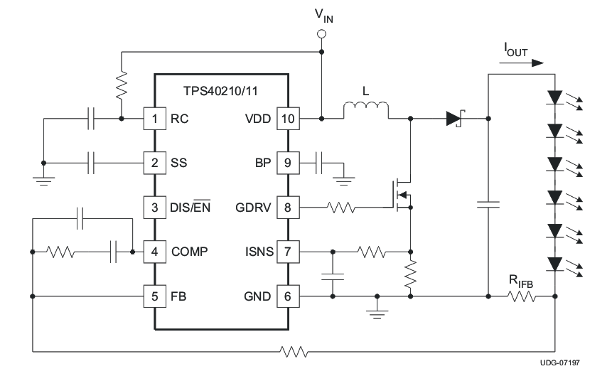
The only difference between the TPS40210 and the TPS40211 is the reference voltage that the error amplifier uses to regulate the output voltage. The TPS40211 uses a 260-mV reference and is intended for applications where the output is actually a current instead of a regulated voltage. A typical example of an application of this type is an LED driver. An example schematic is shown in Figure 29.
 Figure 29. Typical LED Drive Schematic
 The current in the LED string is set by the choice of the resistor RISNS as shown in Equation 31.
Equation 31. 

where
- RIFB is the value of the current sense resistor for the LED string in Ω
- VFB is the reference voltage for the TPS40211 in V (0.260 V typ.)
- IOUT is the desired DC current in the LED string in A