JAJSGE0C JANUARY 2014 – October 2018 TPS40425
PRODUCTION DATA.
- 1 特長
- 2 アプリケーション
- 3 概要
- 4 改訂履歴
- 5 Pin Configuration and Functions
- 6 Specifications
-
7 Detailed Description
- 7.1 Overview
- 7.2 Functional Block Diagram
- 7.3
Feature Description
- 7.3.1 Asynchronous Pulse Injection (API)
- 7.3.2 Adaptive Voltage Scaling (AVS)
- 7.3.3 Switching Frequency and Synchronization
- 7.3.4 Voltage Reference
- 7.3.5 Output Voltage and Remote Sensing Amplifier
- 7.3.6 Current Sensing and Temperature Sensing Modes
- 7.3.7 Current Sensing
- 7.3.8 Temperature Sensing
- 7.3.9 Current Sharing
- 7.3.10 Linear Regulators
- 7.3.11 Power Sequence Between TPS40425 Device and Power Stage
- 7.3.12 PWM Signal
- 7.3.13 Startup and Shutdown
- 7.3.14 Pre-Biased Output Start-up
- 7.3.15 PGOOD Indication
- 7.3.16 Overcurrent Protection
- 7.3.17 Overvoltage/Undervoltage Protection
- 7.3.18 Overtemperature Fault Protection
- 7.3.19 Input Undervoltage Lockout (UVLO)
- 7.3.20 Fault Communication
- 7.3.21 Fault Protection Summary
- 7.4 Device Functional Modes
- 7.5 Programming
- 7.6 Register Maps
- 7.7
Supported PMBus Commands
- 7.7.1 PAGE (00h)
- 7.7.2 OPERATION (01h)
- 7.7.3 ON_OFF_CONFIG (02h)
- 7.7.4 CLEAR_FAULTS (03h)
- 7.7.5 WRITE_PROTECT (10h)
- 7.7.6 STORE_USER_ALL (15h)
- 7.7.7 RESTORE_USER_ALL (16h)
- 7.7.8 CAPABILITY (19h)
- 7.7.9 VOUT_MODE (20h)
- 7.7.10 VIN_ON (35h)
- 7.7.11 VIN_OFF (36h)
- 7.7.12 IOUT_CAL_GAIN (38h)
- 7.7.13 IOUT_CAL_OFFSET (39h)
- 7.7.14 IOUT_OC_FAULT_LIMIT (46h)
- 7.7.15 IOUT_OC_FAULT_RESPONSE (47h)
- 7.7.16 IOUT_OC_WARN_LIMIT (4Ah)
- 7.7.17 OT_FAULT_LIMIT (4Fh)
- 7.7.18 OT_WARN_LIMIT (51h)
- 7.7.19 TON_RISE (61h)
- 7.7.20 STATUS_BYTE (78h)
- 7.7.21 STATUS_WORD (79h)
- 7.7.22 STATUS_VOUT (7Ah)
- 7.7.23 STATUS_IOUT (7Bh)
- 7.7.24 STATUS_TEMPERATURE (7Dh)
- 7.7.25 STATUS_CML (7Eh)
- 7.7.26 STATUS_MFR_SPECIFIC (80h)
- 7.7.27 READ_VOUT (8Bh)
- 7.7.28 READ_IOUT (8Ch)
- 7.7.29 READ_TEMPERATURE_2 (8Eh)
- 7.7.30 PMBus_REVISION (98h)
- 7.7.31 MFR_SPECIFIC_00 (D0h)
- 7.7.32 MFR_SPECIFIC_04 (VREF_TRIM) (D4h)
- 7.7.33 MFR_SPECIFIC_05 (STEP_VREF_MARGIN_HIGH) (D5h)
- 7.7.34 MFR_SPECIFIC_06 (STEP_VREF_MARGIN_LOW) (D6h)
- 7.7.35 MFR_SPECIFIC_07 (PCT_VOUT_FAULT_PG_LIMIT) (D7h)
- 7.7.36 MFR_SPECIFIC_08 (SEQUENCE_TON_TOFF_DELAY) (D8h)
- 7.7.37 MFR_SPECIFIC_16 (COMM_EEPROM_SPARE) (E0h)
- 7.7.38 MFR_SPECIFIC_21 (OPTIONS) (E5h)
- 7.7.39 MFR_SPECIFIC_22 (PWM_OSC_SELECT) (E6h)
- 7.7.40 MFR_SPECIFIC_23 (MASK SMBALERT) (E7h)
- 7.7.41 MFR_SPECIFIC_25 (AVS_CONFIG) (E9h)
- 7.7.42 MFR_SPECIFIC_26 (AVS_ADDRESS) (EAh)
- 7.7.43 MFR_SPECIFIC_27 (AVS_DAC_DEFAULT) (EBh)
- 7.7.44 MFR_SPECIFIC_28 (AVS_CLAMP_HI) (ECh)
- 7.7.45 MFR_SPECIFIC_29 (AVS_CLAMP_LO) (EDh)
- 7.7.46 MFR_SPECIFIC_30 (TEMP_OFFSET) (EEh)
- 7.7.47 MFR_SPECIFIC_32 (API_OPTIONS) (F0h)
- 7.7.48 MFR_SPECIFIC_44 (DEVICE_CODE) (FCh)
-
8 Applications and Implementation
- 8.1 Application Information
- 8.2
Typical Application
- 8.2.1 Dual-Output Application
- 8.2.2 Design Requirements
- 8.2.3
Design Procedure
- 8.2.3.1 Switching Frequency Selection
- 8.2.3.2 Inductor Selection
- 8.2.3.3 Output Capacitor Selection
- 8.2.3.4 Input Capacitor Selection
- 8.2.3.5 VDD, BP5, BP3 Bypass Capacitor
- 8.2.3.6 R-C Snubber
- 8.2.3.7 Current and Temperature Sensor
- 8.2.3.8 Power Sequence Between the TPS40425 Device and Power Stage
- 8.2.3.9 Output Voltage Setting and Frequency Compensation Selection
- 8.2.3.10 Key PMBus Parameter Selection
- 8.2.4 Application Curves
- 9 Power Supply Recommendations
- 10Layout
- 11デバイスおよびドキュメントのサポート
- 12メカニカル、パッケージ、および注文情報
パッケージ・オプション
メカニカル・データ(パッケージ|ピン)
- RHA|40
サーマルパッド・メカニカル・データ
- RHA|40
発注情報
8.2.3.3.1 Output Voltage Deviation During Load Transient
The desired response to a load transient is the first criterion. The output capacitor must supply the load with the required current when not immediately provided by the regulator. When the output capacitor supplies load current, the impedance of the capacitor affects the magnitude of voltage deviation during the transient.
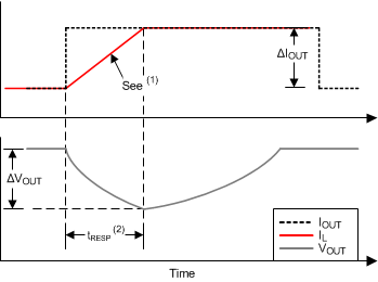
In order to meet the requirements for control loop stability, TPS40425 requires the addition of compensation components in the design of the error amplifier. While these compensation components provide for a stable control loop, they often also reduce the speed with which the regulator can respond to load transients. Figure 22 shows the waveforms of inductor current (IL) and voltage deviation (∆VOUT) during a ∆IOUT load step up. It also shows the response time (tRESP) that inductor current changes from previous load current to the new load current.
The response time tRESP can be calculated using Equation 15 and Equation 16. Usually the cross frequency fCO is set to between one tenth and one fifth of the switching frequency, fSW. In the design the switching frequency is 500 kHz, therefore 50 kHz is used for fCO in the calculation. Equation 18 calculates the minimum required output capacitance COUT(min).


