SLUSBA6B December 2012 – October 2015 TPS51604
PRODUCTION DATA.
- 1 Features
- 2 Applications
- 3 Description
- 4 Revision History
- 5 Pin Configuration and Functions
- 6 Specifications
- 7 Detailed Description
- 8 Application and Implementation
- 9 Power Supply Recommendations
- 10Layout
- 11Device and Documentation Support
- 12Mechanical, Packaging, and Orderable Information
パッケージ・オプション
メカニカル・データ(パッケージ|ピン)
- DSG|8
サーマルパッド・メカニカル・データ
- DSG|8
発注情報
8 Application and Implementation
NOTE
Information in the following applications sections is not part of the TI component specification, and TI does not warrant its accuracy or completeness. TI’s customers are responsible for determining suitability of components for their purposes. Customers should validate and test their design implementation to confirm system functionality.
8.1 Application Information
The TPS51604 driver is optimized for high-frequency CPU VCORE applications. Advanced features such reduced dead-time drive and Auto Zero Crossing are used to optimize efficiency over the entire load range.
8.2 Typical Application
Figure 19 and Figure 20 show a 2-phase design example where TPS51604 device works with the TPS51632 controller and the CSD87381 power block.
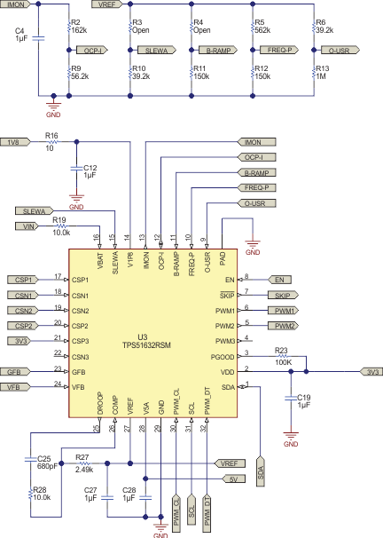 Figure 19. Controller Schematic
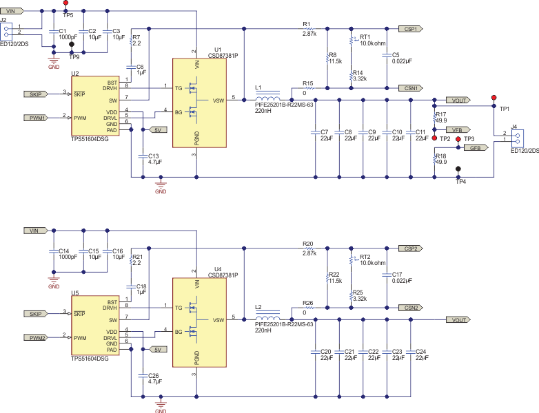 Figure 20. Driver, Power Block, and Output Stage Schematic
8.2.1 Design Requirements
The design example uses the input parameters summarized in Table 2.
Table 2. Design Requirements
| PARAMETER | TEST CONDITIONS | MIN | TYP | MAX | UNIT | |
|---|---|---|---|---|---|---|
| VIN | Input voltage | 6 | 12 | 20 | V | |
| VOUT | Output voltage | 1.2 | V | |||
| VP_P | Output ripple voltage | IOUT = 12 A | 20 | mV | ||
| IOUT | Output current | 0 | 12 | A | ||
| η | Efficiency | IOUT = 12 A, VIN - 12 V | 80% | |||
| fSW | Switching frequency | 1000 | kHz | |||
8.2.2 Detailed Design Procedure
8.2.2.1 Step 1: Select the Input (VDD) Capacitor
A 5-V power supply is suggested for VDD. Placed a ceramic capacitor with a value of 1 uF or greater between VDD and GND.
8.2.2.2 Step 2: Select Boot Capacitor and Boot Resistor
The boot capacitor is the power supply for high-side driver. Place a ceramic capacitor with a value of 0.1 µF or greater between the BST pin and the SW pin.
To reduce the voltage spike on switch node, use a boot resistor with a value of several Ohms in series with boot capacitor to slow the turn-on of high-side FET.
8.2.2.3 Step 3: Establish Connection Between TPS51604 and Controller
Connect the PWM pin of the TPS51604 device to the PWM pin of the controller. The TRIP pins can be used for DCM mode or very-low-power state. Leave the TRIP pin floating if it is not in use.
8.2.2.4 Step 4: Establish Connection Between TPS51604 and the Power Block
Connect the DRVH pin of the TPS51604 device to the gate of the high-side FET of the power block. Connect the DRVL pin of the TPS51604 device to the gate of the low-side FET of the power block. Connect the SW pins of the TPS51604 device to the switch node as required by the high-side driver fo the power block.
8.2.3 Application Curves
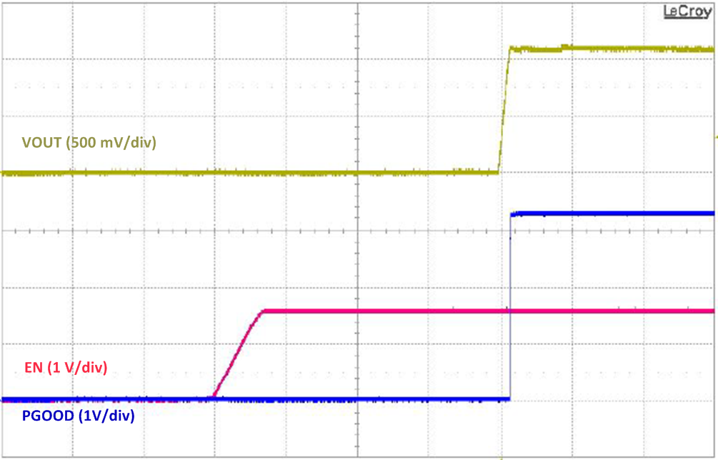
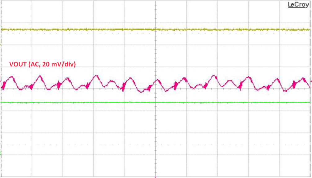
| VIN = 12 V | IOUT = 0 A |
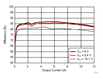
| fSW = 1 MHz |
| VIN = 7.2 V | IOUT = 12 A |