SLUSBN5B August 2013 – July 2015 TPS53515
PRODUCTION DATA.
- 1 Features
- 2 Applications
- 3 Description
- 4 Revision History
- 5 Pin Configuration and Functions
- 6 Specifications
-
7 Detailed Description
- 7.1 Overview
- 7.2 Functional Block Diagram
- 7.3
Feature Description
- 7.3.1 5-V LDO and VREG Start-Up
- 7.3.2 Enable, Soft Start, and Mode Selection
- 7.3.3 Frequency Selection
- 7.3.4 D-CAP3 Control and Mode Selection
- 7.3.5 Power-Good
- 7.3.6 Current Sense and Overcurrent Protection
- 7.3.7 Overvoltage and Undervoltage Protection
- 7.3.8 Out-of-Bounds Operation
- 7.3.9 UVLO Protection
- 7.3.10 Thermal Shutdown
- 7.4 Device Functional Modes
- 8 Application and Implementation
- 9 Power Supply Recommendations
- 10Layout
- 11Device and Documentation Support
- 12Mechanical, Packaging, and Orderable Information
パッケージ・オプション
メカニカル・データ(パッケージ|ピン)
- RVE|28
サーマルパッド・メカニカル・データ
- RVE|28
発注情報
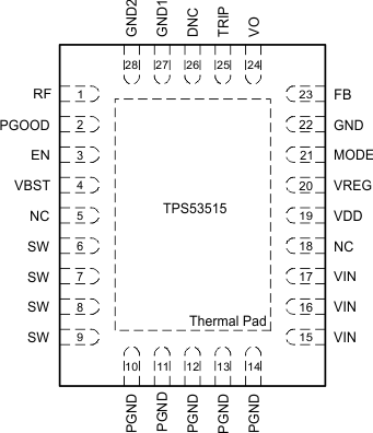
5 Pin Configuration and Functions
RVE Package
28-Pin VQFN-CLIP
Top View

Pin Functions
| PIN | I/O(1) | DESCRIPTION | |
|---|---|---|---|
| NAME | NO. | ||
| DNC | 26 | O | Do not connect. This pin is the output of unused internal circuitry and must be floating. |
| EN | 3 | I | The enable pin turns on the DC-DC switching converter. |
| FB | 23 | I | VOUT feedback input. Connect this pin to a resistor divider between the VOUT pin and GND. |
| GND | 22 | G | This pin is the ground of internal analog circuitry and driver circuitry. Connect GND to the PGND plane with a short trace (For example, connect this pin to the thermal pad with a single trace and connect the thermal pad to PGND pins and PGND plane). |
| GND1 | 27 | I | Connect this pin to ground. GND1 is the input of unused internal circuitry and must connect to ground. |
| GND2 | 28 | I | Connect this pin to ground. GND2 is the input of unused internal circuitry and must connect to ground. |
| MODE | 21 | I | The MODE pin sets the forced continuous-conduction mode (FCCM) or Skip-mode operation. It also selects the ramp coefficient of D-CAP3 mode. |
| NC | 5 | — | Not connected. These pins are floating internally. |
| 18 | |||
| PGND | 10 | G | These ground pins are connected to the return of the internal low-side MOSFET. |
| 11 | |||
| 12 | |||
| 13 | |||
| 14 | |||
| PGOOD | 2 | O | Open-drain power-good status signal which provides startup delay after the FB voltage falls within the specified limits. After the FB voltage moves outside the specified limits, PGOOD goes low within 2 µs. |
| RF | 1 | I | RF is the SW-frequency configuration pin. Connect this pin to a resistor divider between VREG and GND to program different SW frequency settings. |
| SW | 6 | I/O | SW is the output switching terminal of the power converter. Connect this pin to the output inductor. |
| 7 | |||
| 8 | |||
| 9 | |||
| TRIP | 25 | I/O | TRIP is the OCL detection threshold setting pin. ITRIP = 10 µA at room temp, 3000 ppm/°C current is sourced and sets the OCL trip voltage. See the Current Sense and Overcurrent Protection section for detailed OCP setting. |
| VBST | 4 | P | VBST is the supply rail for the high-side gate driver (boost terminal). Connect the bootstrap capacitor from this pin to the SW node. Internally connected to VREG via bootstrap PMOS switch. |
| VDD | 19 | P | Power-supply input pin for controller. Input of the VREG LDO. The input range is from 4.5 to 25 V. |
| VIN | 15 | P | VIN is the conversion power-supply input pins. |
| 16 | |||
| 17 | |||
| VREG | 20 | O | VREG is the 5-V LDO output. This voltage supplies the internal circuitry and gate driver. |
| VO | 24 | I | VOUT voltage input to the controller. |
(1) I = Input, O = Output, P = Supply, G = Ground