SLUSAS9B NOVEMBER 2013 – December 2014 TPS53915
PRODUCTION DATA.
- 1 Features
- 2 Applications
- 3 Description
- 4 Revision History
- 5 Pin Configuration and Functions
- 6 Specifications
-
7 Detailed Description
- 7.1 Overview
- 7.2 Functional Block Diagrams
- 7.3
Feature Description
- 7.3.1 Powergood
- 7.3.2 D-CAP3 Control and Mode Selection
- 7.3.3 D-CAP3 Mode
- 7.3.4 Sample and Hold Circuitry
- 7.3.5 Adaptive Zero-Crossing
- 7.3.6 Forced Continuous-Conduction Mode
- 7.3.7 Current Sense and Overcurrent Protection
- 7.3.8 Overvoltage and Undervoltage Protection
- 7.3.9 Out-Of-Bounds Operation (OOB)
- 7.3.10 UVLO Protection
- 7.3.11 Thermal Shutdown
- 7.4 Device Functional Modes
- 7.5
Programming
- 7.5.1 The PMBus General Descriptions
- 7.5.2 PMBus Slave Address Selection
- 7.5.3 PMBus Address Selection
- 7.5.4 Supported Formats
- 7.5.5 Supported PMBus Commands
- 7.5.6 CLEAR_FAULTS [03h] (Send Byte)
- 7.5.7 STORE_DEFAULT_ALL [11h] (Send Byte)
- 7.5.8 RESTORE_DEFAULT_ALL [12h] (Send Byte)
- 7.5.9 STATUS_WORD [79h] (Read Word)
- 7.5.10 CUSTOM_REG (MFR_SPECIFIC_00) [D0h] (R/W Byte)
- 7.5.11 DELAY_CONTROL (MFR_SPECIFIC_01) [D1h] (R/W Byte)
- 7.5.12 MODE_SOFT_START_CONFIG (MFR_SPECIFIC_02) [D2h] (R/W Byte)
- 7.5.13 FREQUENCY_CONFIG (MFR_SPECIFIC_03) [D3h] (R/W Byte)
- 7.5.14 VOUT_ADJUSTMENT (MFR_SPECIFIC_04) [D4h] (R/W Byte)
- 7.5.15 Output Voltage Fine Adjustment Soft Slew Rate
- 7.5.16 VOUT_MARGIN (MFR_SPECIFIC_05) [D5h] (R/W Byte)
- 7.5.17 Output Voltage Margin Adjustment Soft-Slew Rate
- 7.5.18 UVLO_THRESHOLD (MFR_SPECIFIC_06) [D6h]
- 8 Application and Implementation
- 9 Power Supply Recommendations
- 10Layout
- 11Device and Documentation Support
- 12Mechanical, Packaging, and Orderable Information
パッケージ・オプション
メカニカル・データ(パッケージ|ピン)
- RVE|28
サーマルパッド・メカニカル・データ
- RVE|28
発注情報
8 Application and Implementation
NOTE
Information in the following applications sections is not part of the TI component specification, and TI does not warrant its accuracy or completeness. TI’s customers are responsible for determining suitability of components for their purposes. Customers should validate and test their design implementation to confirm system functionality.
8.1 Application Information
The TPS53915 device is a high-efficiency, single-channel, synchronous-buck converter. The device suits low-output voltage point-of-load applications with 12-A or lower output current in computing and similar digital consumer applications.
8.2 Typical Application
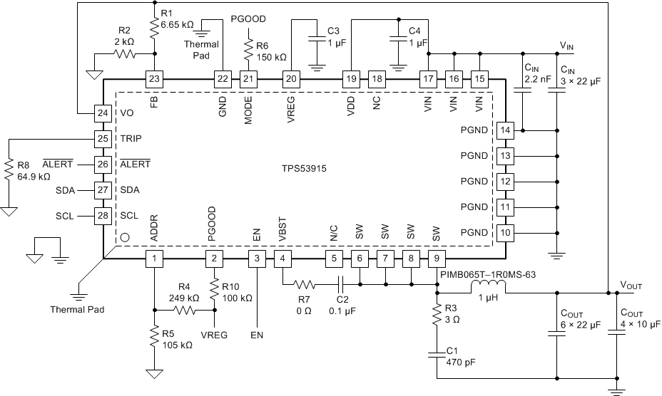 Figure 52. Typical Application Circuit Diagram
8.2.1 Design Requirements
This design uses the parameters listed in Table 19.
Table 19. Design Example Specifications
| PARAMETER | TEST CONDITIONS | MIN | TYP | MAX | UNIT | ||
|---|---|---|---|---|---|---|---|
| INPUT CHARACTERISTICS | |||||||
| VIN | Voltage range | 5 | 12 | 18 | V | ||
| IMAX | Maximum input current | V IN = 5 V, I OUT = 8 A | 2.5 | A | |||
| No load input current | V IN = 12 V, I OUT = 0 A with auto skip mode | 1 | mA | ||||
| OUTPUT CHARACTERISTICS | |||||||
| VOUT | Output voltage | 1.2 | V | ||||
| Output voltage regulation | Line regulation, 0.2% 5 V ≤ V IN ≤ – 14 V with FCCM | 0.2% | |||||
| Load regulation, 0.5% V IN = 12 V, 0 A ≤ I OUT ≤ 8 A with FCCM | 0.5% | ||||||
| VRIPPLE | Output voltage ripple | V IN = 12 V, I OUT = 8 A with FCCM | 10 | mV PP | |||
| ILOAD | Output load current | 0 | 8 | A | |||
| IOVER | Output over current | 11 | |||||
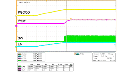
| tSS | Soft-start time | 1 | ms | ||||
| SYSTEM CHARACTERISTICS | |||||||
| fSW | Switching frequency | 500 | kHz | ||||
| η | Peak efficiency | V IN = 12 V, V OUT = 1.2 V ,I OUT = 4 A | 88.5% | ||||
| Full load efficiency | V IN = 12 V, V OUT = 1.2 V , I OUT = 8 A | 88.9% | |||||
| TA | Operating temperature | 25 | ºC | ||||
8.2.2 Detailed Design Procedure
The external components selection is a simple process using D-CAP3 Mode. Select the external components using the following steps.
8.2.2.1 Choose the Switching Frequency
The default switching frequency (fSW) is pre-set at 400 kHz. The switching frequency can be changed through PMBus function MFR_SPECIFIC_03 (see Table 13).
8.2.2.2 Choose the Operation Mode
Select the operation mode using Table 3.
8.2.2.3 Choose the Inductor
Determine the inductance value to set the ripple current at approximately ¼ to ½ of the maximum output current. Larger ripple current increases output ripple voltage, improves signal-to-noise ratio, and helps to stabilize operation.
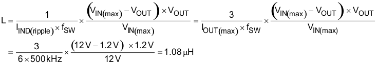
The inductor requires a low DCR to achieve good efficiency. The inductor also requires enough room above peak inductor current before saturation. The peak inductor current is estimated using Equation 7.

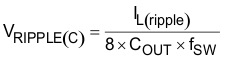
8.2.2.4 Choose the Output Capacitor
The output capacitor selection is determined by output ripple and transient requirement. When operating in CCM, the output ripple has two components as shown in Equation 8. Equation 9 and Equation 10 define these components.


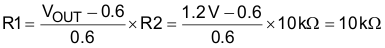
8.2.2.5 Determine the Value of R1 and R2
The output voltage is programmed by the voltage-divider resistors, R1 and R2, shown in Equation 11. Connect R1 between the VFB pin and the output, and connect R2 between the VFB pin and GND. The recommended R2 value is from 1 kΩ to 20 kΩ. Determine R1 using Equation 11.
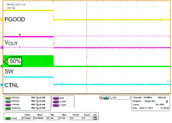
8.2.3 Application Curves
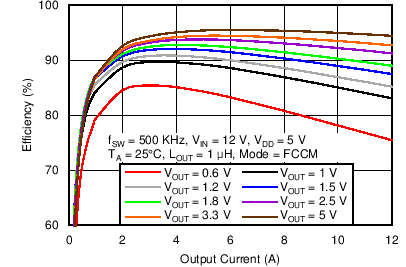 Figure 53. Efficiency vs. Output Current
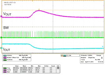
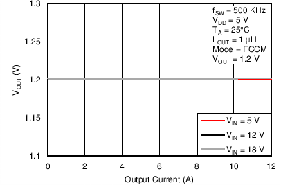 Figure 55. Output Voltage vs. Output Current
| ILOAD = 6 A |
| ILOAD from 0 A to 6 A | ||
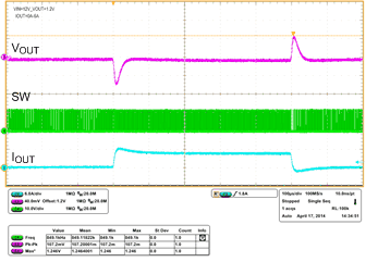
| ILOAD from 0 A to 6A to 0 A | ||
| ILOAD = 6 A |
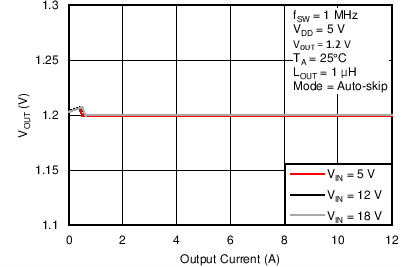 Figure 54. Output Voltage vs. Output Current
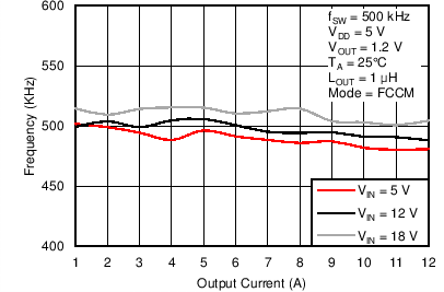 Figure 56. Switching Frequency vs. Output Current
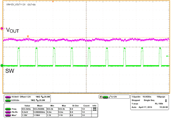
| ILOAD = 6 A |
| ILOAD from 6A to 0 A | ||
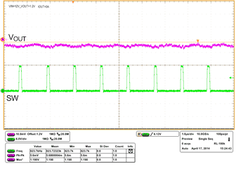
| ILOAD = 0 A |
| Preset VOUT = 0.5 V | ||