SLUSAS9B NOVEMBER 2013 – December 2014 TPS53915
PRODUCTION DATA.
- 1 Features
- 2 Applications
- 3 Description
- 4 Revision History
- 5 Pin Configuration and Functions
- 6 Specifications
-
7 Detailed Description
- 7.1 Overview
- 7.2 Functional Block Diagrams
- 7.3
Feature Description
- 7.3.1 Powergood
- 7.3.2 D-CAP3 Control and Mode Selection
- 7.3.3 D-CAP3 Mode
- 7.3.4 Sample and Hold Circuitry
- 7.3.5 Adaptive Zero-Crossing
- 7.3.6 Forced Continuous-Conduction Mode
- 7.3.7 Current Sense and Overcurrent Protection
- 7.3.8 Overvoltage and Undervoltage Protection
- 7.3.9 Out-Of-Bounds Operation (OOB)
- 7.3.10 UVLO Protection
- 7.3.11 Thermal Shutdown
- 7.4 Device Functional Modes
- 7.5
Programming
- 7.5.1 The PMBus General Descriptions
- 7.5.2 PMBus Slave Address Selection
- 7.5.3 PMBus Address Selection
- 7.5.4 Supported Formats
- 7.5.5 Supported PMBus Commands
- 7.5.6 CLEAR_FAULTS [03h] (Send Byte)
- 7.5.7 STORE_DEFAULT_ALL [11h] (Send Byte)
- 7.5.8 RESTORE_DEFAULT_ALL [12h] (Send Byte)
- 7.5.9 STATUS_WORD [79h] (Read Word)
- 7.5.10 CUSTOM_REG (MFR_SPECIFIC_00) [D0h] (R/W Byte)
- 7.5.11 DELAY_CONTROL (MFR_SPECIFIC_01) [D1h] (R/W Byte)
- 7.5.12 MODE_SOFT_START_CONFIG (MFR_SPECIFIC_02) [D2h] (R/W Byte)
- 7.5.13 FREQUENCY_CONFIG (MFR_SPECIFIC_03) [D3h] (R/W Byte)
- 7.5.14 VOUT_ADJUSTMENT (MFR_SPECIFIC_04) [D4h] (R/W Byte)
- 7.5.15 Output Voltage Fine Adjustment Soft Slew Rate
- 7.5.16 VOUT_MARGIN (MFR_SPECIFIC_05) [D5h] (R/W Byte)
- 7.5.17 Output Voltage Margin Adjustment Soft-Slew Rate
- 7.5.18 UVLO_THRESHOLD (MFR_SPECIFIC_06) [D6h]
- 8 Application and Implementation
- 9 Power Supply Recommendations
- 10Layout
- 11Device and Documentation Support
- 12Mechanical, Packaging, and Orderable Information
パッケージ・オプション
メカニカル・データ(パッケージ|ピン)
- RVE|28
サーマルパッド・メカニカル・データ
- RVE|28
発注情報
6 Specifications
6.1 Absolute Maximum Ratings
over operating free-air temperature range (unless otherwise noted)(1)| MIN | MAX | UNIT | |||
|---|---|---|---|---|---|
| Input voltage range(2) | EN | –0.3 | 7.7 | V | |
| SW | DC | –3 | 30 | ||
| Transient < 10 ns | –5 | 32 | |||
| VBST | –0.3 | 36 | |||
| VBST(3) | –0.3 | 6 | |||
| VBST when transient < 10 ns | 38 | ||||
| VDD | –0.3 | 28 | |||
| VIN | –0.3 | 30 | |||
| ADDR, FB, MODE, SDA, SCL, VO | –0.3 | 6 | |||
| Output voltage range | PGOOD | –0.3 | 7.7 | V | |
| ALERT, TRIP, VREG | –0.3 | 6 | |||
| Junction Temperature, TJ | –40 | 150 | °C | ||
| Storage Temperature, Tstg | –55 | 150 | °C | ||
(1) Stresses beyond those listed under Absolute Maximum Ratings may cause permanent damage to the device. These are stress ratings only, and functional operation of the device at these or any other conditions beyond those indicated under Recommended Operating Conditions is not implied. Exposure to absolute-maximum-rated conditions for extended periods my affect device reliability.
(2) All voltages are with respect to network ground terminal.
(3) Voltage values are with respect to the SW terminal.
6.2 ESD Ratings
| VALUE | UNIT | |||
|---|---|---|---|---|
| V(ESD) | Electrostatic discharge | Human-body model (HBM), per ANSI/ESDA/JEDEC JS-001(1) | ±2500 | V |
| Charged-device model (CDM), per JEDEC specification JESD22-C101(2) | ±1500 | |||
(1) JEDEC document JEP155 states that 500-V HBM allows safe manufacturing with a standard ESD control process.
(2) JEDEC document JEP157 states that 250-V CDM allows safe manufacturing with a standard ESD control process.
6.3 Recommended Operating Conditions
over operating free-air temperature range (unless otherwise noted)| MIN | MAX | UNIT | |||
|---|---|---|---|---|---|
| Input voltage range | EN | –0.1 | 7 | V | |
| SW | –3 | 27 | |||
| VBST | –0.1 | 28 | |||
| VBST(1) | –0.1 | 5.5 | |||
| VDD | 4.5 | 25 | |||
| VIN | 1.5 | 18 | |||
| ADDR, FB, MODE, SDA, SCL, VO | –0.1 | 5.5 | |||
| Output voltage range | PGOOD | –0.1 | 7 | V | |
| ALERT, TRIP, VREG | –0.1 | 5.5 | |||
| TA | Operating free-air temperature | –40 | 85 | °C | |
(1) Voltage values are with respect to the SW pin.
6.4 Thermal Information
| THERMAL METRIC(1) | TPS53915 | UNIT | |
|---|---|---|---|
| RVE | |||
| 28 PINS | |||
| θJA | Junction-to-ambient thermal resistance(2) | 37.5 | °C/W |
| θJCtop | Junction-to-case (top) thermal resistance(3) | 34.1 | |
| θJB | Junction-to-board thermal resistance(4) | 18.1 | |
| ψJT | Junction-to-top characterization parameter(5) | 1.8 | |
| ψJB | Junction-to-board characterization parameter(6) | 18.1 | |
| θJCbot | Junction-to-case (bottom) thermal resistance(7) | 2.2 | |
(1) For more information about traditional and new thermal metrics, see the IC Package Thermal Metrics application report, SPRA953.
(2) The junction-to-ambient thermal resistance under natural convection is obtained in a simulation on a JEDEC-standard, high-K board, as specified in JESD51-7, in an environment described in JESD51-2a.
(3) The junction-to-case (top) thermal resistance is obtained by simulating a cold plate test on the package top. No specific JEDEC-standard test exists, but a close description can be found in the ANSI SEMI standard G30-88.
(4) The junction-to-board thermal resistance is obtained by simulating in an environment with a ring cold plate fixture to control the PCB temperature, as described in JESD51-8.
(5) The junction-to-top characterization parameter, ψJT, estimates the junction temperature of a device in a real system and is extracted from the simulation data for obtaining RθJA, using a procedure described in JESD51-2a (sections 6 and 7).
(6) The junction-to-board characterization parameter, ψJB, estimates the junction temperature of a device in a real system and is extracted from the simulation data for obtaining RθJA, using a procedure described in JESD51-2a (sections 6 and 7).
(7) The junction-to-case (bottom) thermal resistance is obtained by simulating a cold plate test on the exposed (power) pad. No specific JEDEC standard test exists, but a close description can be found in the ANSI SEMI standard G30-88.
6.5 Electrical Characteristics
over operating free-air temperature range, VREG = 5 V, VEN = 5 V (unless otherwise noted)| PARAMETER | TEST CONDITIONS | MIN | TYP | MAX | UNIT | |
|---|---|---|---|---|---|---|
| SUPPLY CURRENT | ||||||
| IVDD | VDD bias current | TA = 25°C, No load Power conversion enabled (no switching) |
1350 | 1850 | µA | |
| IVDDSTBY | VDD standby current | TA = 25°C, No load Power conversion disabled |
850 | 1150 | µA | |
| IVIN(leak) | VIN leakage current | VEN = 0 V | 0.5 | µA | ||
| VREF OUTPUT | ||||||
| VVREF | Reference voltage | FB w/r/t GND, TA = 25°C | 597 | 600 | 603 | mV |
| VVREFTOL | Reference voltage tolerance | FB w/r/t GND, TJ = 0°C to 85°C | –0.6% | 0.5% | ||
| FB w/r/t GND, TJ = –40°C to 85°C | –0.7% | 0.5% | ||||
| OUTPUT VOLTAGE | ||||||
| IFB | FB input current | VFB = 600 mV | 50 | 100 | nA | |
| IVODIS | VO discharge current | VVO = 0.5 V, Power Conversion Disabled | 10 | 12 | 15 | mA |
| INTERNAL DAC REFERENCE | ||||||
| VDACTOL1 | DAC voltage tolerance 1 | FB w/r/t GND, 0°C ≤ TA ≤ 85°C, with certain VOUT_ADJUSTMENT settings only (2) | –4.8 | 4.8 | mV | |
| VDACTOL2 | DAC voltage tolerance 2 | FB w/r/t GND, 0°C ≤ TA ≤ 85°C, with certain VOUT_MARGIN settings only (3) | –4.8 | 4.8 | mV | |
| VDACTOL3 | DAC voltage tolerance 3 | FB w/r/t GND, 0°C ≤ TA ≤ 85°C, with VOUT_ADJUSTMENT=0Dh and VOUT_MARGIN=70h for 5% | –4.8 | 4.8 | mV | |
| VDACTOL4 | DAC voltage tolerance 4 | FB w/r/t GND, 0°C ≤ TA ≤ 85°C, with VOUT_ADJUSTMENT=13h and VOUT_MARGIN=07h for -5% | –4.8 | 4.8 | mV | |
| SMPS FREQUENCY | ||||||
| fSW | VO switching frequency | VIN = 12 V, VVO = 3.3 V, FS<2:0> = 000 | 250 | kHz | ||
| VIN = 12 V, VVO = 3.3 V, FS<2:0> = 001 | 300 | |||||
| VIN = 12 V, VVO = 3.3 V, FS<2:0> = 010 | 400 | |||||
| VIN = 12 V, VVO = 3.3 V, FS<2:0> = 011 | 500 | |||||
| VIN = 12 V, VVO = 3.3 V, FS<2:0> = 100 | 600 | |||||
| VIN = 12 V, VVO = 3.3 V, FS<2:0> = 101 | 750 | |||||
| VIN = 12 V, VVO = 3.3 V, FS<2:0> = 110 | 850 | |||||
| VIN = 12 V, VVO = 3.3 V, FS<2:0> = 111 | 1000 | |||||
| tON(min) | Minimum on-time | TA = 25°C(1) | 60 | ns | ||
| tOFF(min) | Minimum off-time | TA = 25°C | 175 | 240 | 310 | ns |
| INTERNAL BOOTSTRAP SW | ||||||
| VF | Forward Voltage | VVREG–VBST, TA = 25°C, IF = 10 mA | 0.15 | 0.25 | V | |
| IVBST | VBST leakage current | TA = 25°C, VVBST = 33 V, VSW = 28 V | 0.01 | 1.5 | µA | |
| LOGIC THRESHOLD | ||||||
| VENH | EN enable threshold voltage | 1.3 | 1.4 | 1.5 | V | |
| VENL | EN disable threshold voltage | 1.1 | 1.2 | 1.3 | V | |
| VENHYST | EN hysteresis voltage | 0.22 | V | |||
| VENLEAK | EN input leakage current | –1 | 0 | 1 | µA | |
| SOFT-START | ||||||
| tSS | Soft-start time | SST <1:0> = 00 | 1 | ms | ||
| SST <1:0> = 01 | 2 | |||||
| SST <1:0> = 10 | 4 | |||||
| SST <1:0> = 11 | 8 | |||||
| POWERGOOD COMPARATOR | ||||||
| VPGTH | PGOOD threshold | PGOOD in from higher | 104% | 108% | 111% | |
| PGOOD in from lower | 89% | 92% | 96% | |||
| PGOOD out to higher | 113% | 116% | 120% | |||
| PGOOD out to lower | 80% | 84% | 87% | |||
| tPGDLY | PGOOD delay time | Delay for PGOOD going in PGD<2:0>=000 | 165 | 256 | 320 | μs |
| Delay for PGOOD going in PGD<2:0>=001 | 409 | 512 | 614 | μs | ||
| Delay for PGOOD going in PGD<2:0>=010 | 0.819 | 1.024 | 1.228 | ms | ||
| Delay for PGOOD going in PGD<2:0>=011 | 1.638 | 2.048 | 2.458 | ms | ||
| Delay for PGOOD going in PGD<2:0>=100 | 3.276 | 4.096 | 4.915 | ms | ||
| Delay for PGOOD going in PGD<2:0>=101 | 6.553 | 8.192 | 9.83 | ms | ||
| Delay for PGOOD going in PGD<2:0>=110 | 13.104 | 16.38 | 19.656 | ms | ||
| Delay for PGOOD going in PGD<2:0>=111 | 105 | 131 | 157 | ms | ||
| Delay tolerance for PGOOD coming out | 2 | µs | ||||
| IPG | PGOOD sink current | VPGOOD = 0.5 V | 4 | 6 | mA | |
| IPGLK | PGOOD leakage current | VPGOOD = 5.0 V | –1 | 0 | 1 | µA |
| POWER-ON DELAY | ||||||
| tPODLY | Power-on delay time | Delay from enable to switching POD<2:0>=000 | 356 | µs | ||
| Delay from enable to switching POD<2:0>=001 | 612 | µs | ||||
| Delay from enable to switching POD<2:0>=010 | 1.124 | ms | ||||
| Delay from enable to switching POD<2:0>=011 | 2.148 | ms | ||||
| Delay from enable to switching POD<2:0>=100 | 4.196 | ms | ||||
| Delay from enable to switching POD<2:0>=101 | 8.292 | ms | ||||
| Delay from enable to switching POD<2:0>=110 | 16.48 | ms | ||||
| Delay from enable to switching POD<2:0>=111 | 32.86 | ms | ||||
| CURRENT DETECTION | ||||||
| RTRIP | TRIP pin resistance range | 20 | 70 | kΩ | ||
| IOCL | Current limit threshold, valley | RTRIP = 52.3 kΩ | 10.1 | 12.0 | 13.9 | A |
| RTRIP = 38 kΩ | 7.2 | 9.1 | 11.0 | |||
| IOCLN | Negative current limit threshold, valley | RTRIP = 52.3 kΩ | –15.3 | –11.9 | –8.5 | A |
| RTRIP = 38 kΩ | –12 | –9 | –6 | |||
| VZC | Zero cross detection offset | 0 | mV | |||
| PROTECTIONS | ||||||
| VVREGUVLO | VREG undervoltage-lockout (UVLO) threshold voltage | Wake-up | 3.25 | 3.34 | 3.41 | V |
| Shutdown | 3.00 | 3.12 | 3.19 | |||
| VVDDUVLO | VDD UVLO threshold voltage | Wake-up (default) | 4.15 | 4.25 | 4.35 | V |
| Shutdown | 3.95 | 4.05 | 4.15 | |||
| VOVP | Overvoltage-protection (OVP) threshold voltage | OVP detect voltage | 116% | 120% | 124% | |
| tOVPDLY | OVP propagation delay | With 100-mV overdrive | 300 | ns | ||
| VUVP | Undervoltage-protection (UVP) threshold voltage | UVP detect voltage | 64% | 68% | 71% | |
| tUVPDLY | UVP delay | UVP filter delay | 1 | ms | ||
| THERMAL SHUTDOWN | ||||||
| TSDN | Thermal shutdown threshold(1) | Shutdown temperature | 140 | °C | ||
| Hysteresis | 40 | |||||
| LDO VOLTAGE | ||||||
| VREG | LDO output voltage | VIN = 12 V, ILOAD = 10 mA | 4.65 | 5 | 5.45 | V |
| VDOVREG | LDO low droop drop-out voltage | VIN = 4.5 V, ILOAD = 30 mA, TA = 25°C | 365 | mV | ||
| ILDOMAX | LDO over-current limit | VIN = 12 V, TA = 25°C | 170 | 200 | mA | |
| INTERNAL MOSFETS | ||||||
| RDS(on)H | High-side MOSFET on-resistance | TA = 25°C | 13.8 | 15.5 | mΩ | |
| RDS(on)L | Low-side MOSFET on-resistance | TA = 25°C | 5.9 | 7.0 | mΩ | |
| PMBus SCL and SDA INPUT BUFFER LOGIC THRESHOLDS | ||||||
| VIL-PMBUS | SCL and SDA low-level input voltage(1) | 0°C ≤ TJ ≤ 85°C | 0.8 | V | ||
| VIH-PMBUS | SCL and SDA high-level input voltage(1) | 0°C ≤ TJ ≤ 85°C | 2.1 | V | ||
| VHY-PMBUS | SCL and SDA hysteresis voltage(1) | 0°C ≤ TJ ≤ 85°C | 240 | mV | ||
| PMBus SDA and ALERT OUTPUT PULLDOWN | ||||||
| VOL1-PMBUS | SDA and ALERT low-level output voltage(1) | VDDPMBus = 5.5 V, RPULLUP = 1.1 kΩ, 0°C ≤ TJ ≤ 85°C |
0.4 | V | ||
| VOL2-PMBUS | SDA and ALERT low-level output voltage(1) | VDDPMBus = 3.6 V, RPULLUP = 0.7 kΩ, 0°C ≤ TJ ≤ 85°C |
0.4 | V | ||
(1) Specified by design. Not production tested.
(2) Tested at these VOUT_ADJUSTMENT settings: -9.0%, -8.25%, -5.25%, -2.25%, 0.0%, 3.00%, 6.00%, 9.0%
(3) Tested at these VOUT_MARGIN settings: -11.62%, -10.74%, -7.06%, -3.15%, 0%, 3.7%, 7.74%, 12.05%
6.6 Typical Characteristics
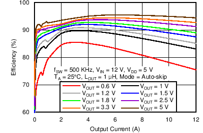 Figure 1. Efficiency vs. Output Current
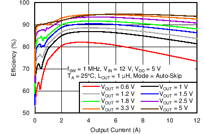 Figure 3. Efficiency vs. Output Current
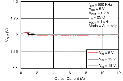 Figure 5. Output Voltage vs. Output Current
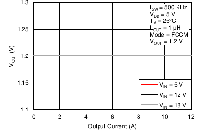 Figure 7. Output Voltage vs. Output Current
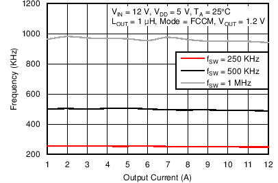 Figure 9. Switching Frequency vs. Output Current
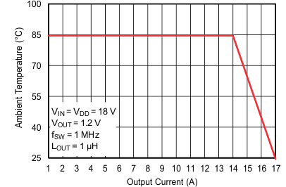 Figure 11. Safe Operating Area, VOUT = 1.2 V
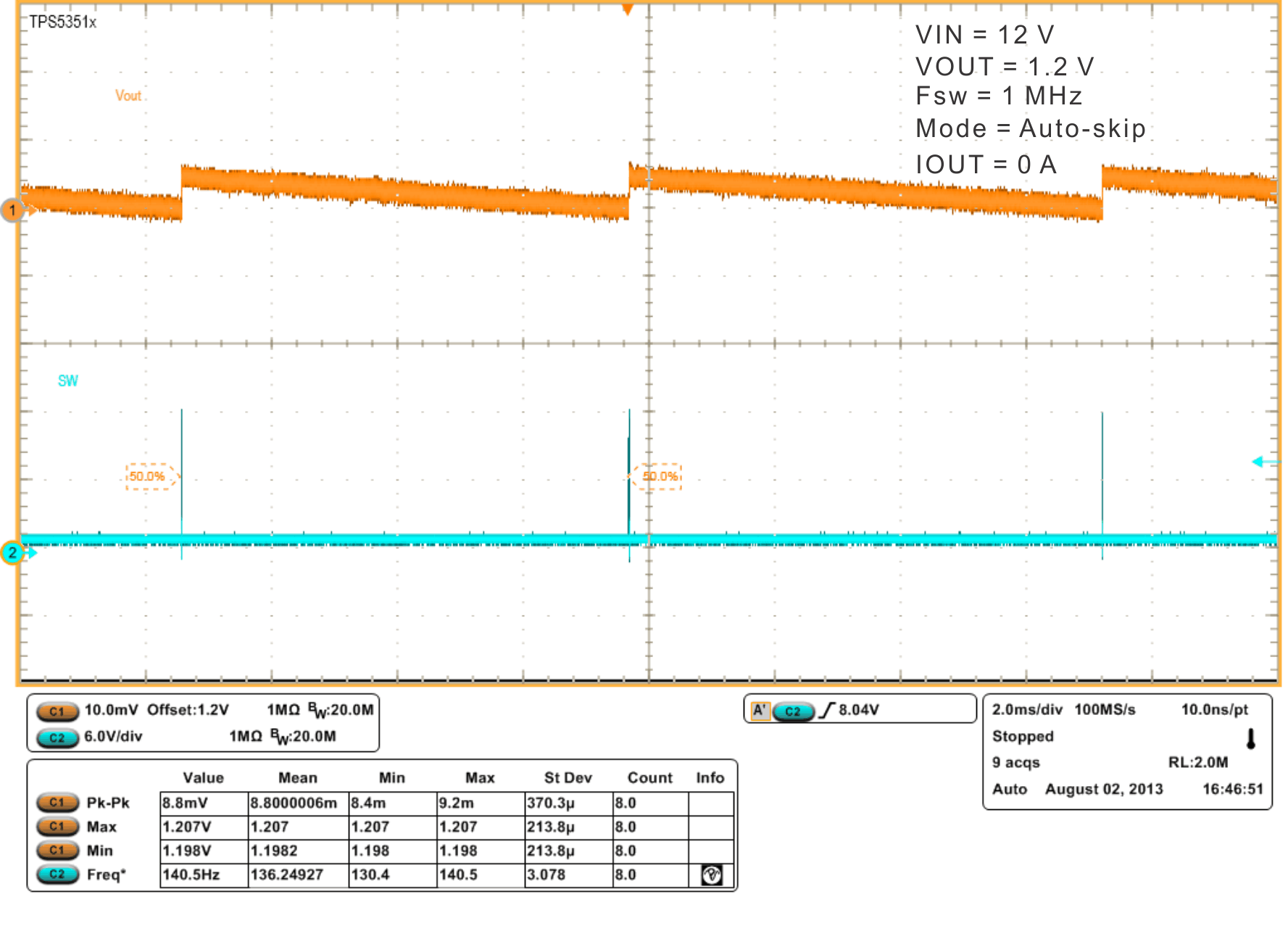 Figure 13. Auto-Skip Steady-State Operation
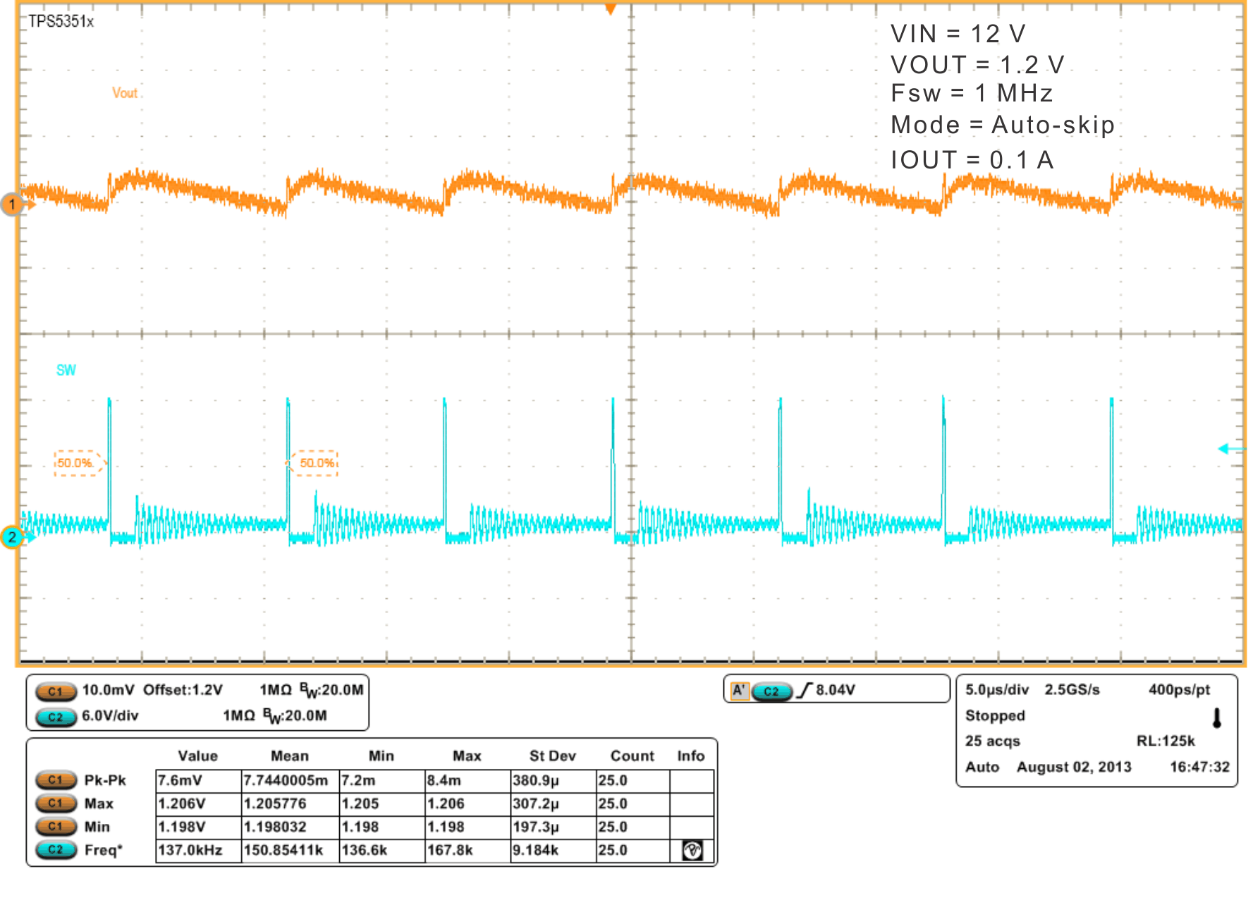 Figure 15. Auto-Skip Steady-State Operation
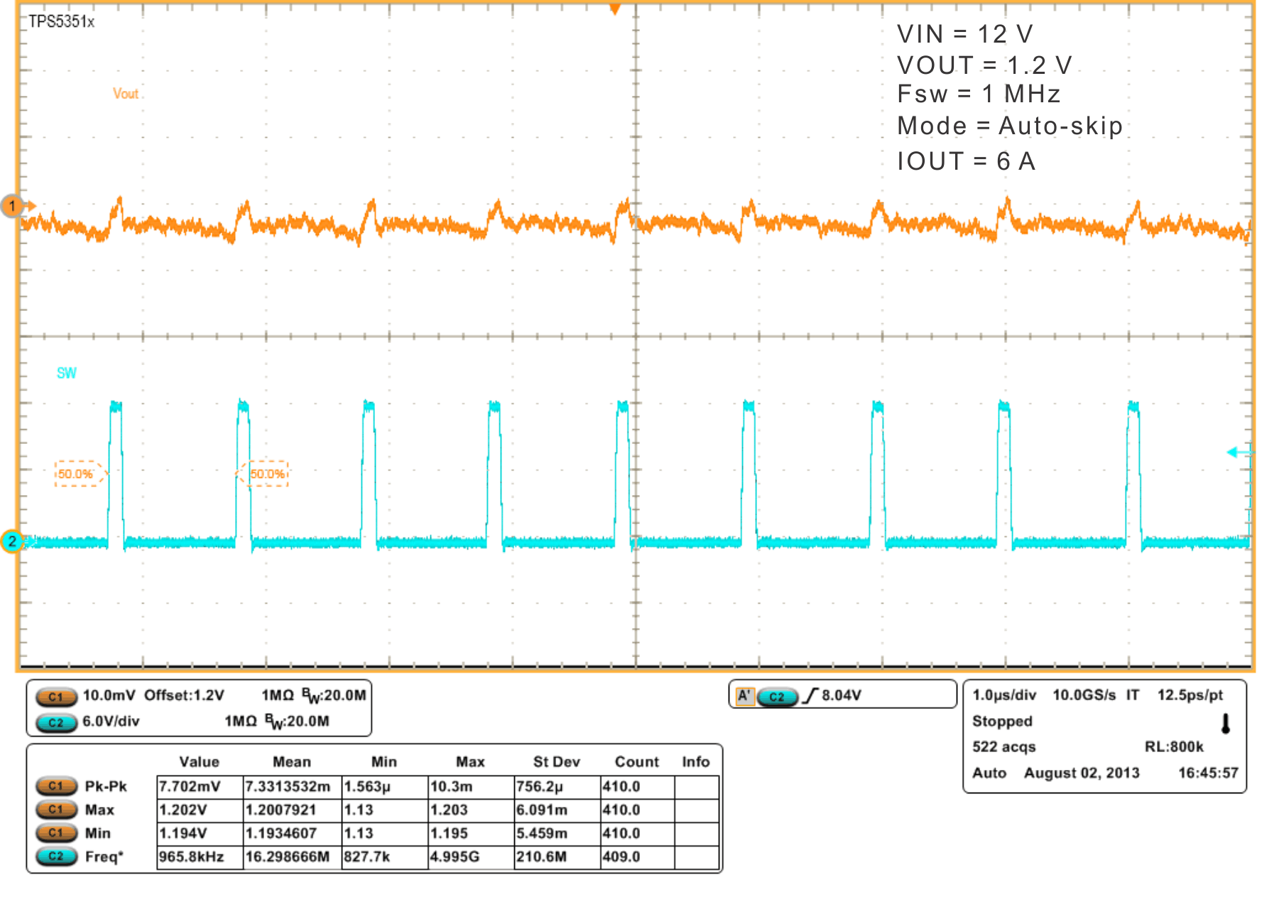 Figure 17. Auto-Skip Steady-State Operation
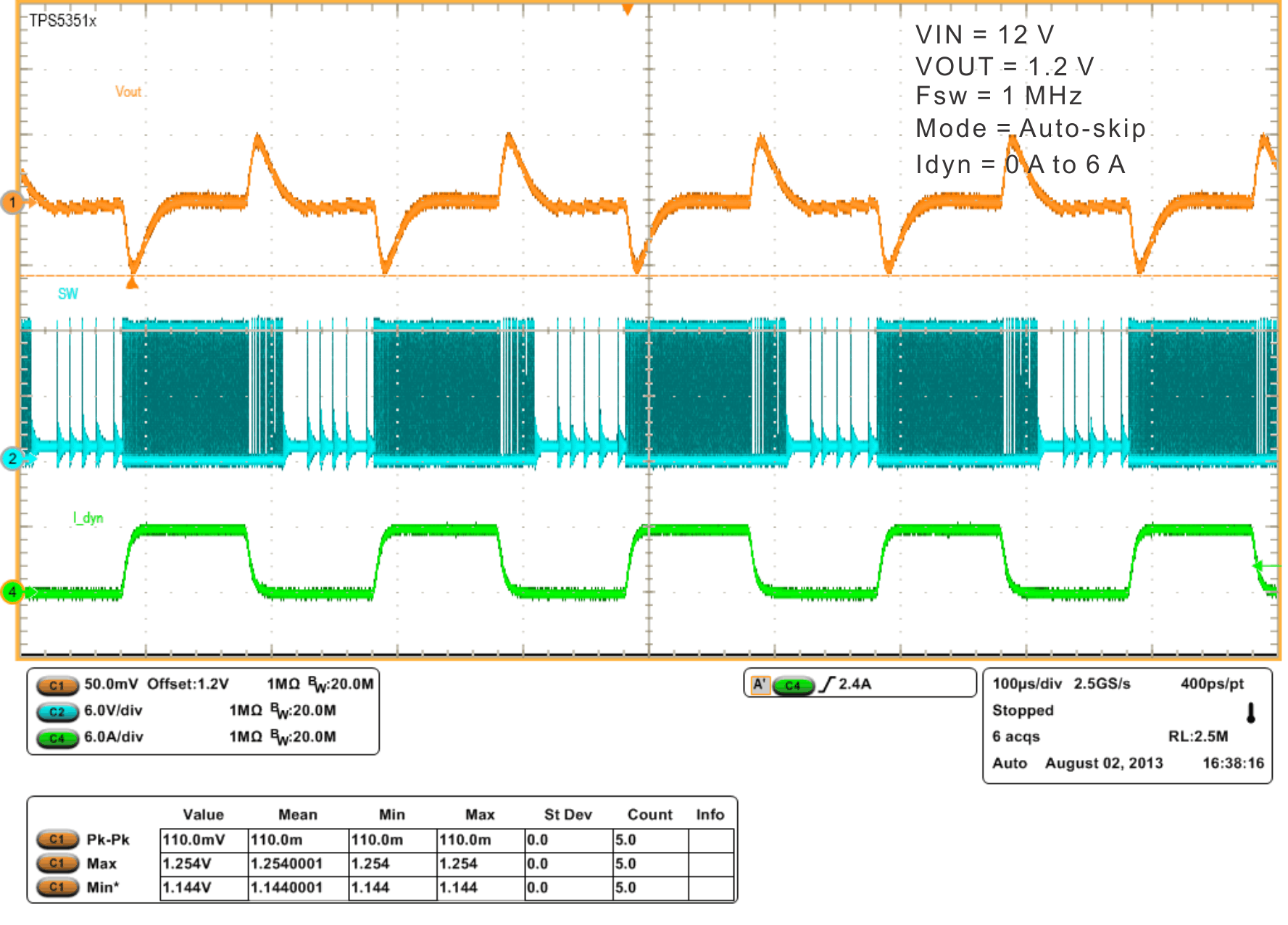 Figure 19. Auto-Skip Mode Load Transient
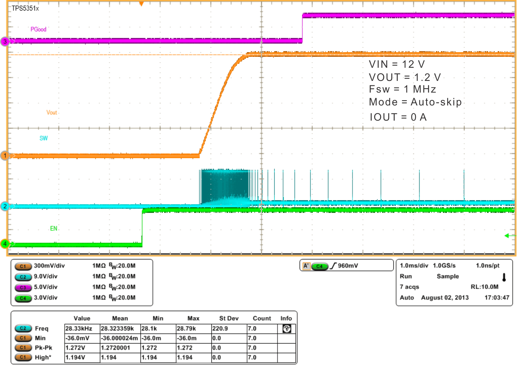 Figure 21. Start-Up
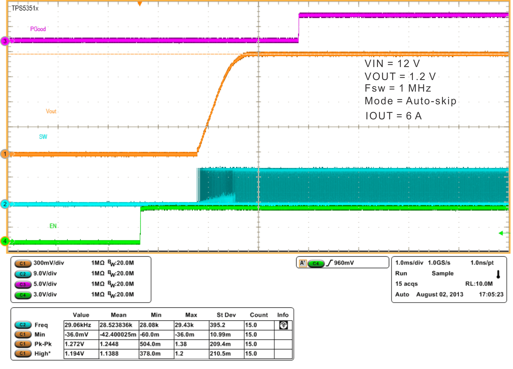 Figure 23. Start-Up
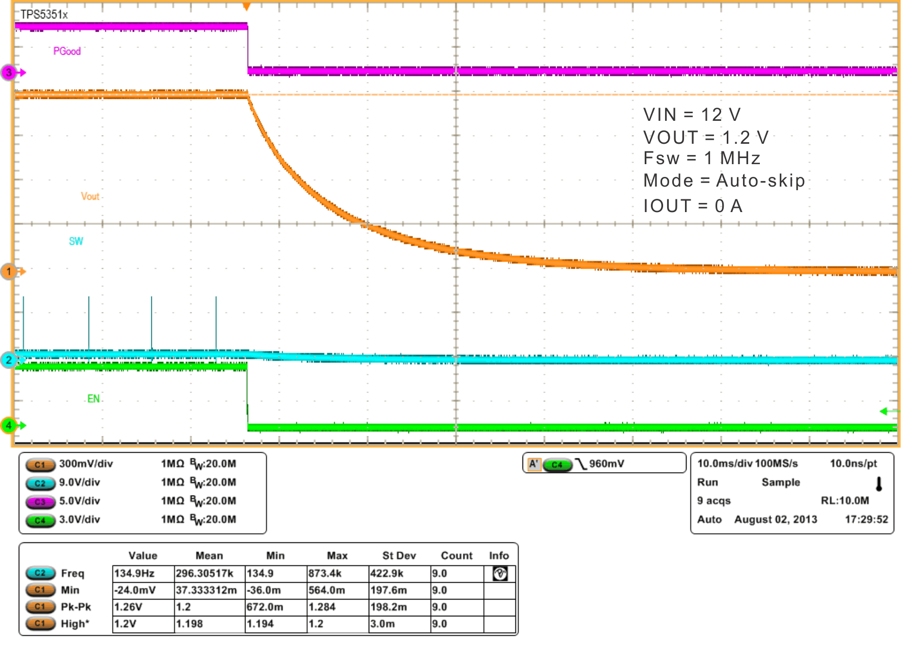 Figure 25. Shutdown Operation
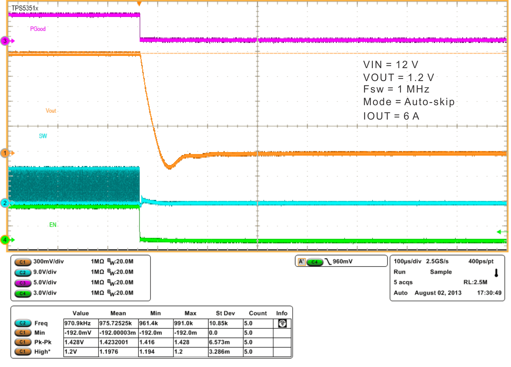 Figure 27. Shutdown Operation
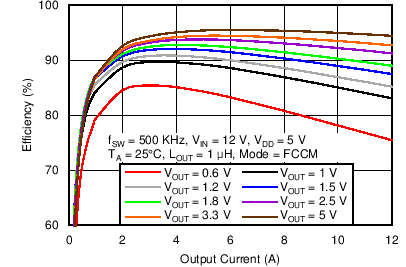 Figure 2. Efficiency vs. Output Current
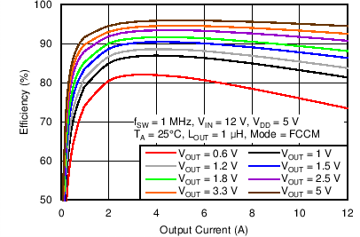 Figure 4. Efficiency vs. Output Current
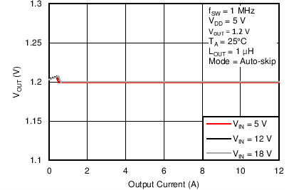 Figure 6. Output Voltage vs. Output Current
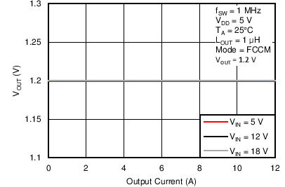 Figure 8. Output Voltage vs. Output Current
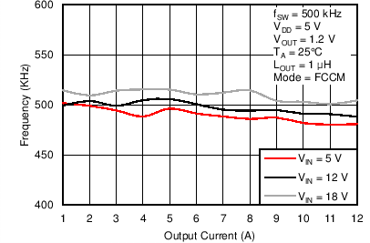 Figure 10. Switching Frequency vs. Output Current
 Figure 12. Safe Operating Area, VOUT = 5 V
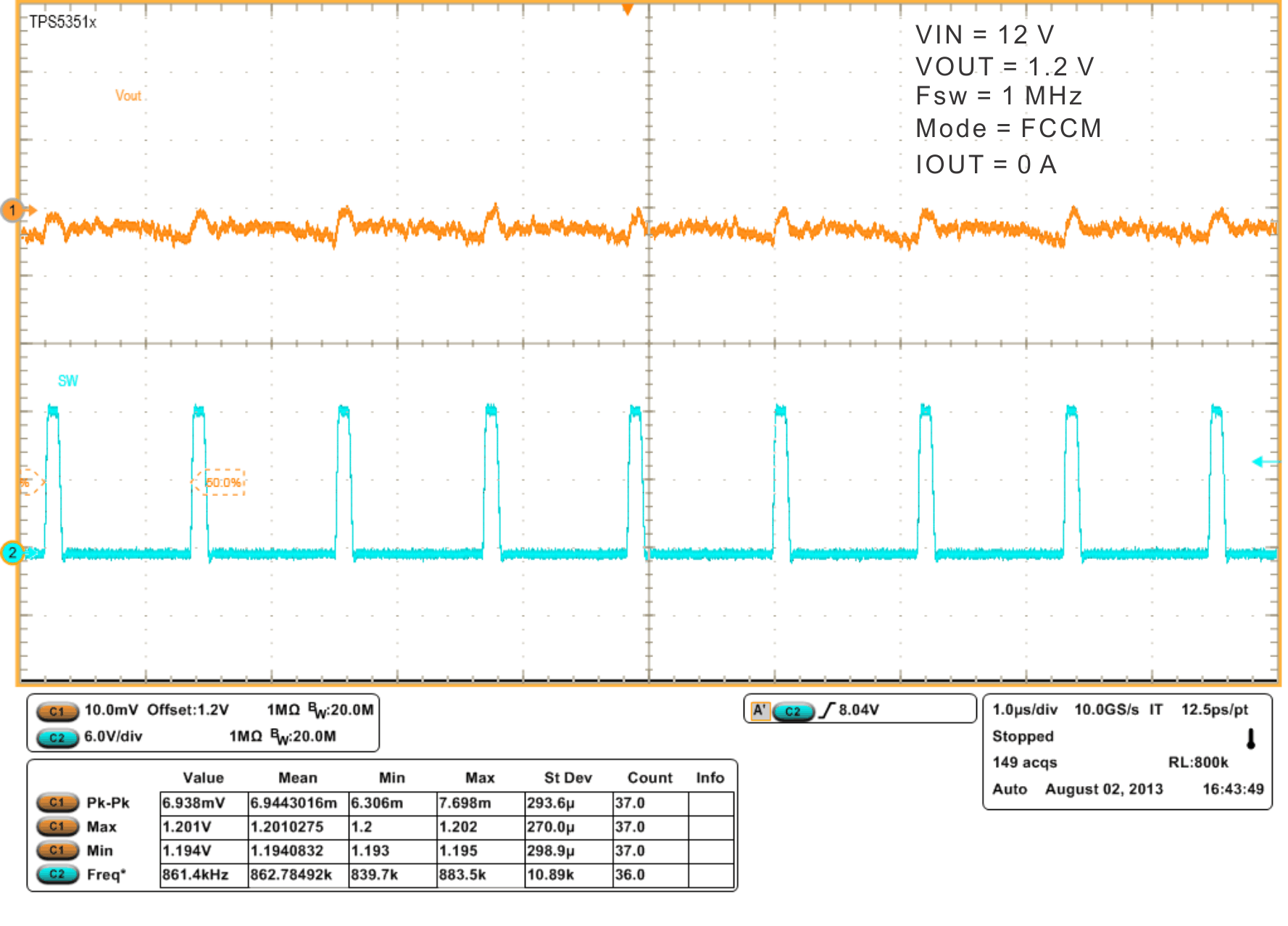 Figure 14. FCCM Steady-State Operation
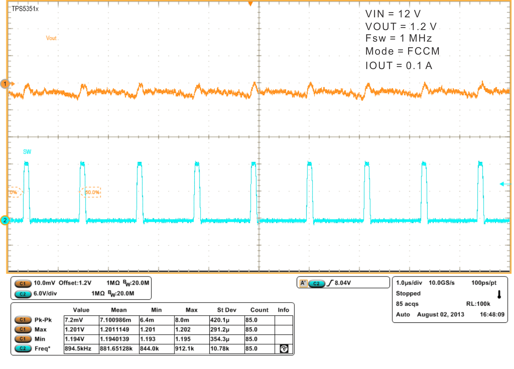 Figure 16. FCCM Steady-State Operation
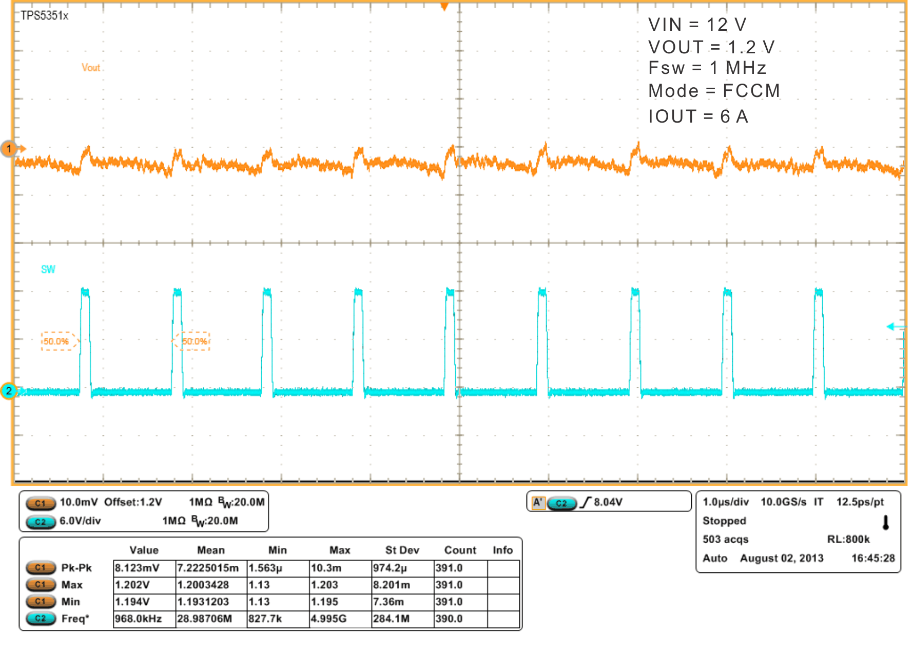 Figure 18. FCCM Steady-State Operation
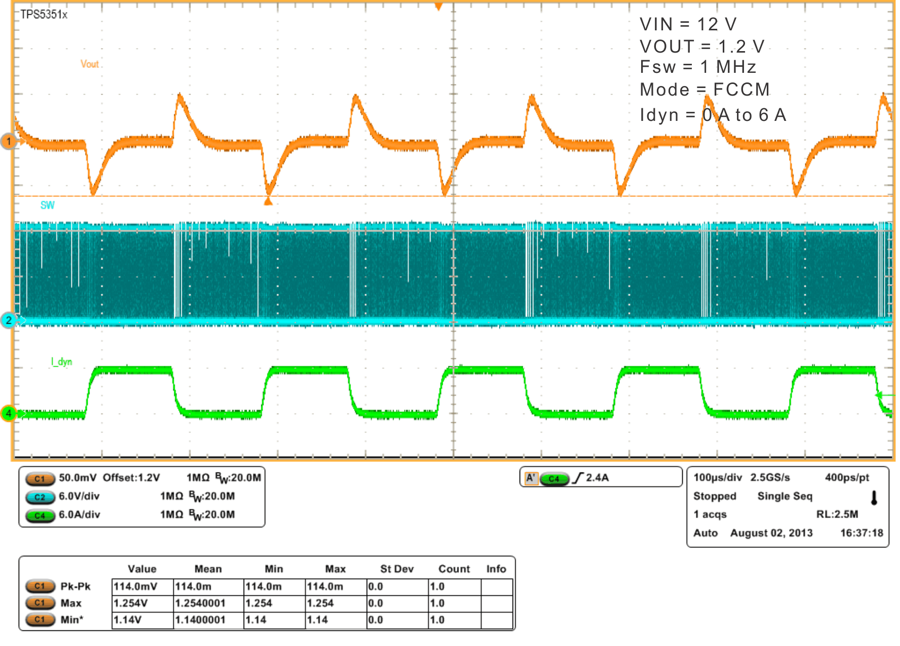 Figure 20. FCCM Mode Load Transient
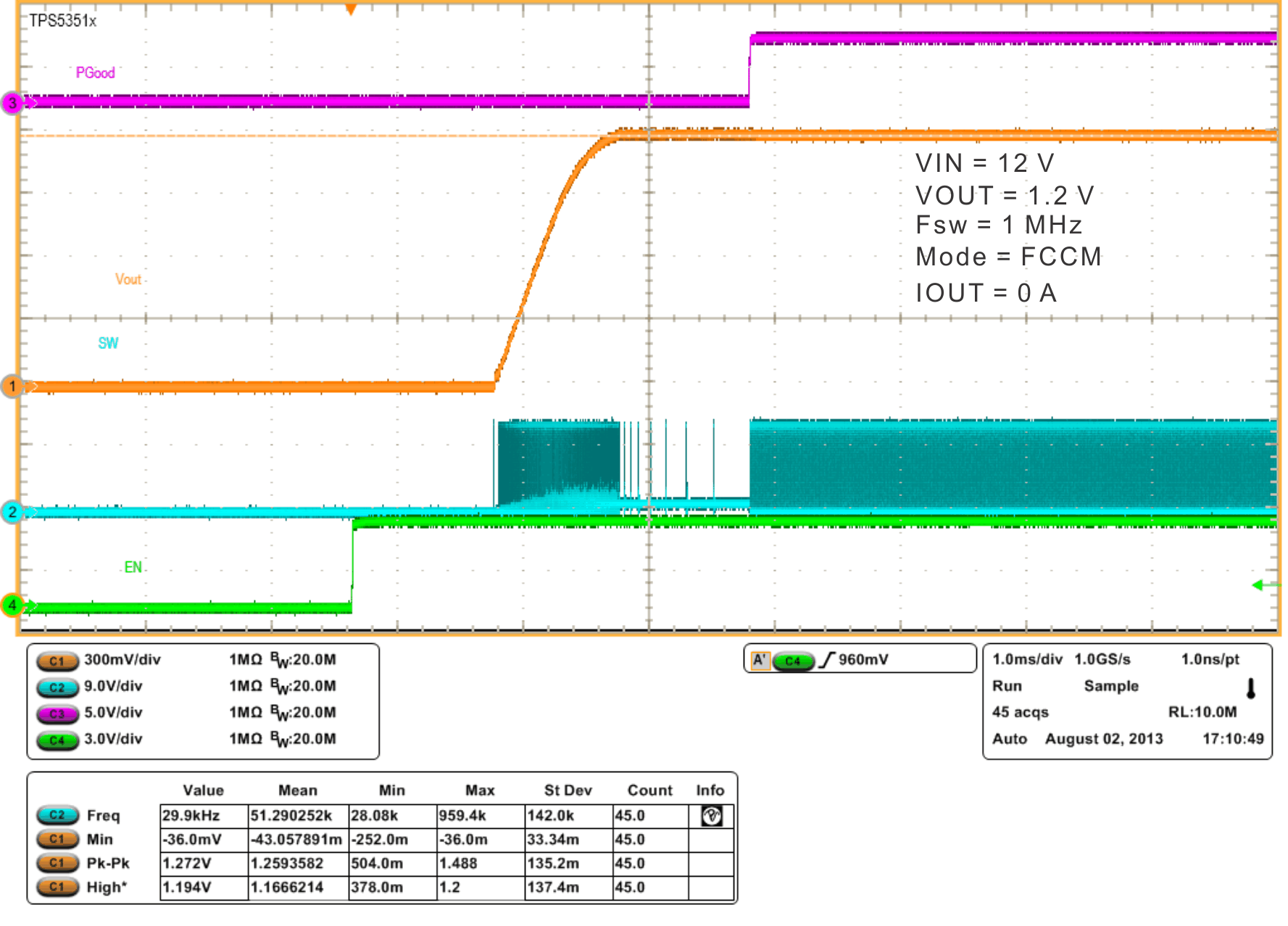 Figure 22. Start-Up
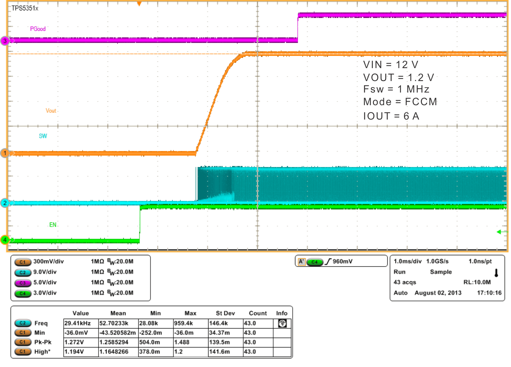 Figure 24. Start-Up
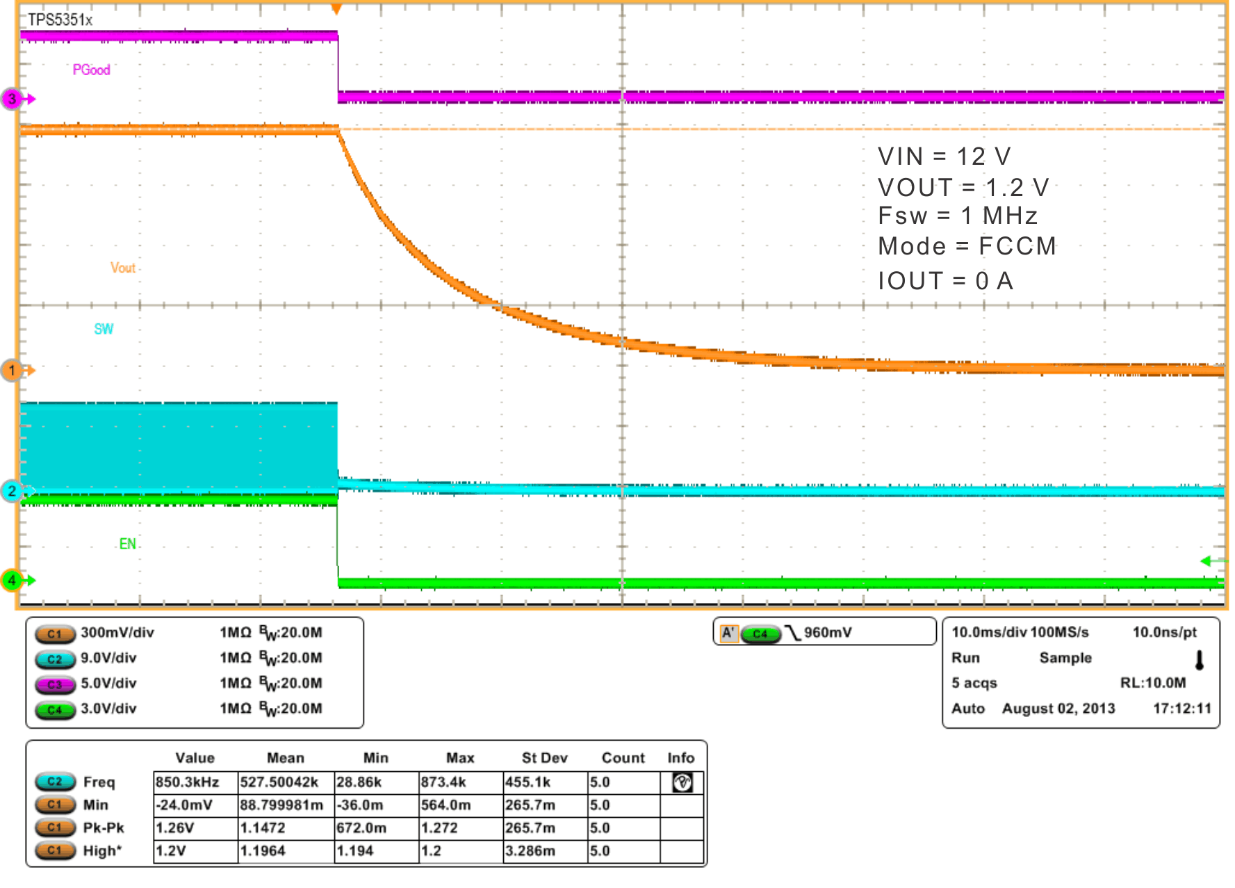 Figure 26. Shutdown Operation
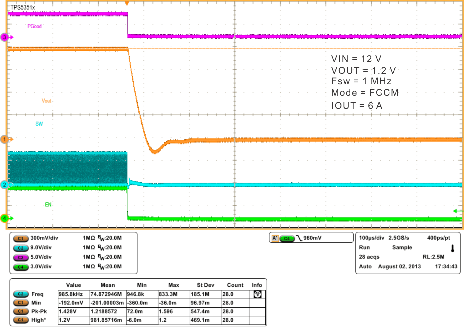 Figure 28. Shutdown Operation
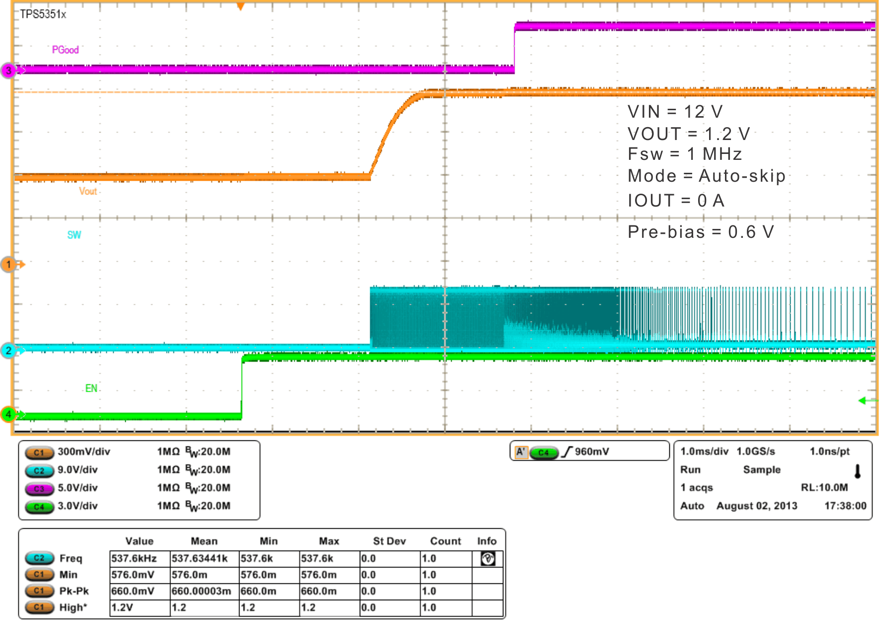 Figure 29. Pre-Bias Operation
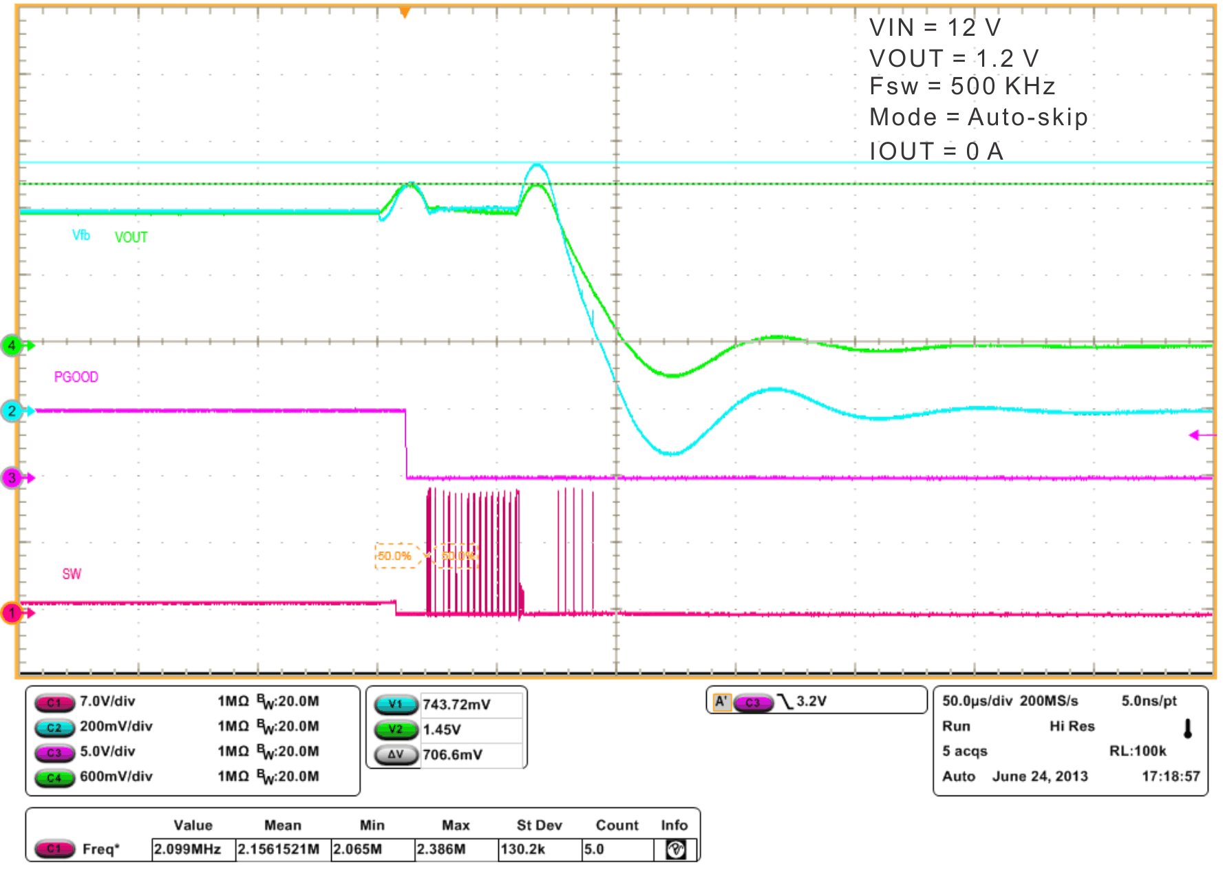 Figure 30. Overvoltage Protection
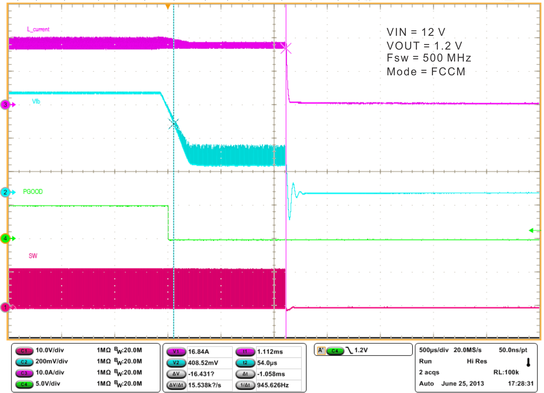 Figure 31. Overcurrent Protection
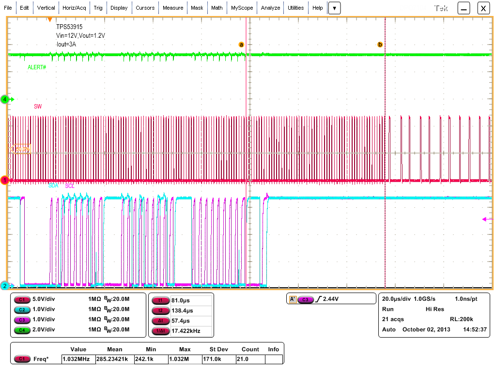 Figure 33. 1 MHz to 250 KHz
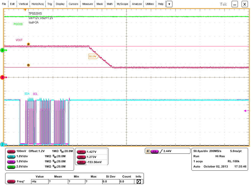 Figure 35. VOUT(adj) = 6%, VOMH = 12% to 0%
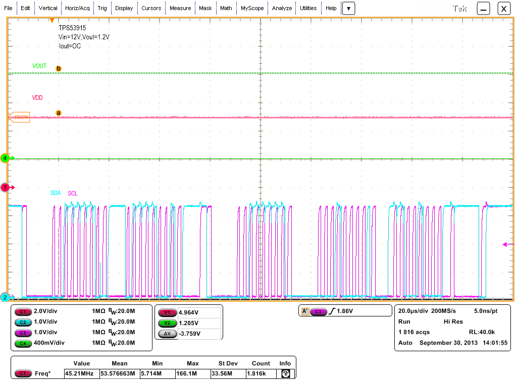 Figure 32. I2C READ (Address=31d, Cmd=0x79): ACK 0x10C8. IOC = 15 A
 Figure 34. 31d_FFh_FFh
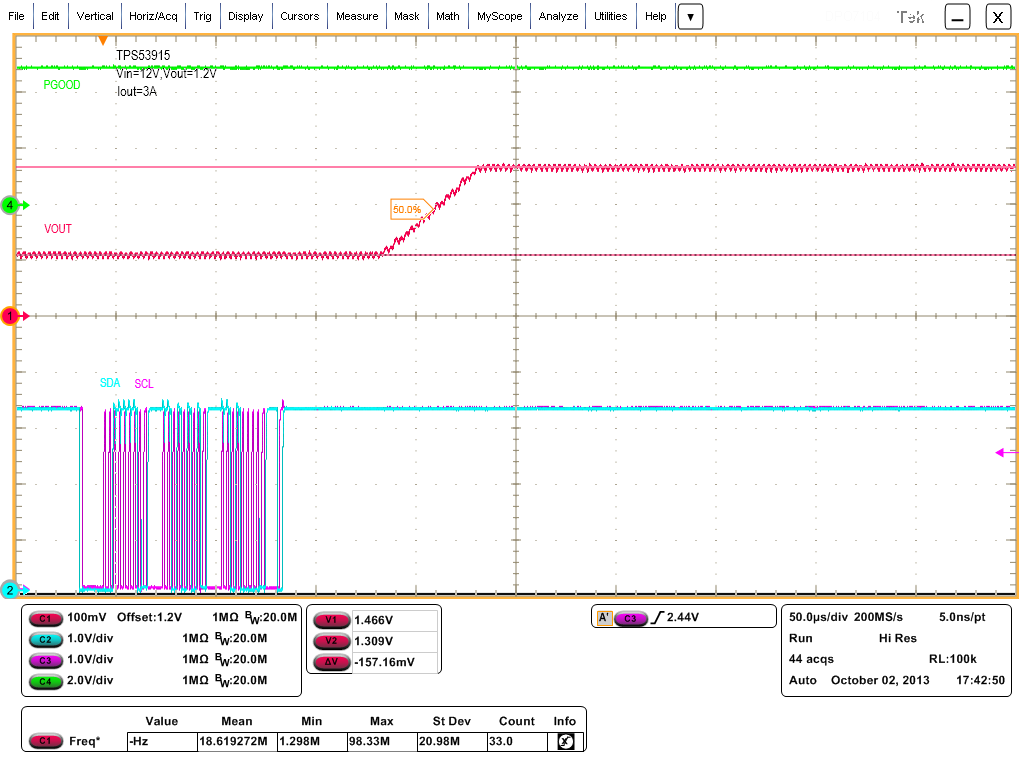 Figure 36. VOUT(adj) = 9%, VOMH = 0% to 12%
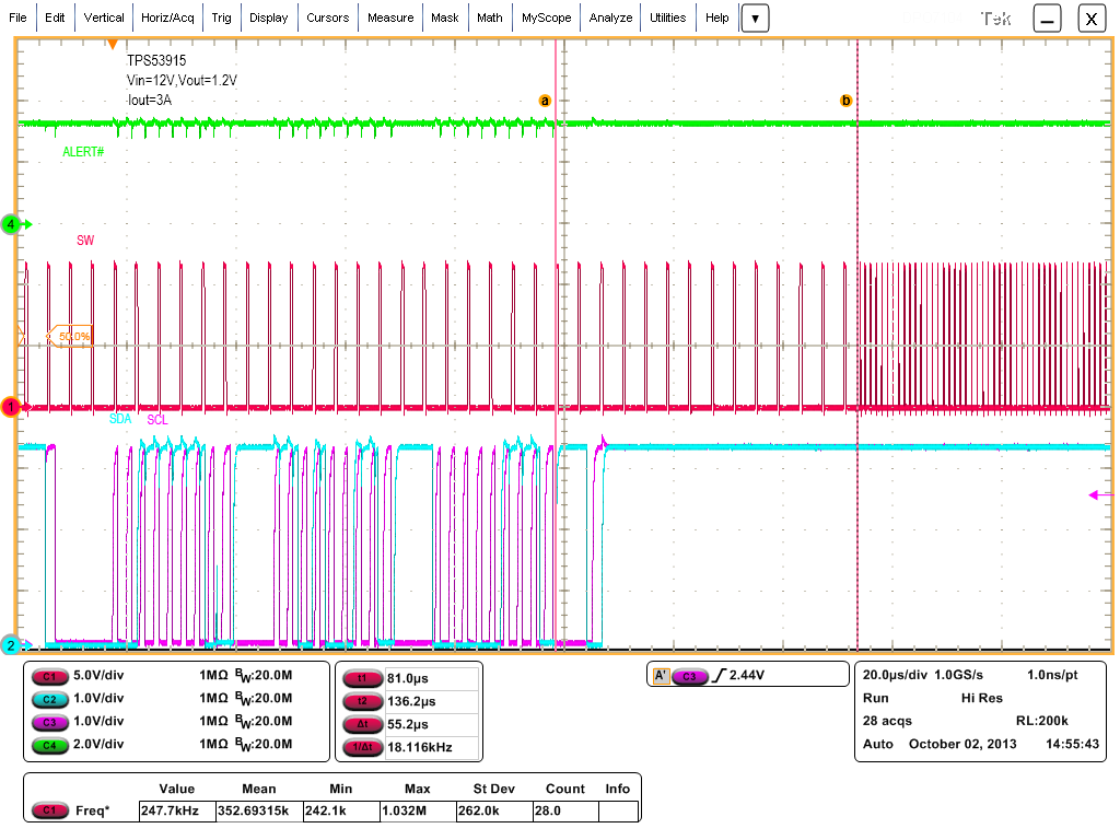 Figure 37. 250 kHz to MHz
6.7 Thermal Performance
fSW = 500 kHz, VIN = 12 V, VOUT = 5 V, IOUT = 12 A, COUT = 10 × 22 µF (1206, 6.3V, X5R), RBOOT = 0 Ω, SNB = 3 Ω + 470 pF Inductor: LOUT = 1 µH, PCMC135T-1R0MF, 12.6 mm × 13.8 mm × 5 mm, 2.1 mΩ (typ)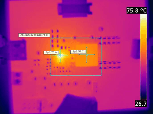 Figure 38. SP1: 75.6℃ (TPS53915), SP2: 57.7℃ (Inductor)