JAJSCQ2B November   2016  – June 2018 TPS54200 , TPS54201

PRODUCTION DATA.  

  1. 特長
  2. アプリケーション
  3. 概要
    1.     Device Images
      1.      概略回路図
      2.      ADIMでの優れた深調光機能
  4. 改訂履歴
  5. 概要(続き)
  6. Pin Configuration and Functions
    1.     Pin Functions
  7. Specifications
    1. 7.1 Absolute Maximum Ratings
    2. 7.2 ESD Ratings
    3. 7.3 Recommended Operating Conditions
    4. 7.4 Thermal Information
    5. 7.5 Electrical Characteristics
    6. 7.6 Timing Requirements
    7. 7.7 Switching Characteristics
    8. 7.8 Typical Characteristics
  8. Detailed Description
    1. 8.1 Overview
    2. 8.2 Functional Block Diagram
    3. 8.3 Feature Description
      1. 8.3.1  Fixed-Frequency PWM Control
      2. 8.3.2  Error Amplifier
      3. 8.3.3  Slope Compensation and Output Current
      4. 8.3.4  Input Undervoltage Lockout
      5. 8.3.5  Voltage Reference
      6. 8.3.6  Setting LED Current
      7. 8.3.7  Internal Soft Start
      8. 8.3.8  Bootstrap Voltage (BOOT)
      9. 8.3.9  Overcurrent Protection
        1. 8.3.9.1 High-Side MOSFET Overcurrent Protection
        2. 8.3.9.2 Low-Side MOSFET Overcurrent Protection
        3. 8.3.9.3 Low-Side MOSFET Reverse Overcurrent Protection
      10. 8.3.10 Fault Protection
        1. 8.3.10.1 LED-Open Protection
        2. 8.3.10.2 LED Short Protection
        3. 8.3.10.3 Sense-Resistor Short Protection
        4. 8.3.10.4 Sense-Resistor Open Protection
        5. 8.3.10.5 Overvoltage Protection
        6. 8.3.10.6 Thermal Shutdown
    4. 8.4 Device Functional Modes
      1. 8.4.1 Enable and Disable Device
      2. 8.4.2 Mode Detection
      3. 8.4.3 Analog Dimming Mode Operation
      4. 8.4.4 PWM Dimming-Mode Operation
  9. Application and Implementation
    1. 9.1 Application Information
    2. 9.2 Typical Application
      1. 9.2.1 TPS5420x 12-V Input, 1.5-A, 3-Piece IR LED Driver With Analog Dimming
        1. 9.2.1.1 Design Requirements
        2. 9.2.1.2 Detailed Design Procedure
          1. 9.2.1.2.1 Inductor Selection
          2. 9.2.1.2.2 Input Capacitor Selection
          3. 9.2.1.2.3 Output Capacitor Selection
          4. 9.2.1.2.4 FB Pin RC Filter Selection
          5. 9.2.1.2.5 Sense Resistor Selection
        3. 9.2.1.3 Application Curves
      2. 9.2.2 TPS5420x 24-V Input, 1-A, 4-Piece WLED Driver With PWM Dimming
        1. 9.2.2.1 Design Requirements
        2. 9.2.2.2 Detailed Design Procedure
          1. 9.2.2.2.1 Inductor Selection
          2. 9.2.2.2.2 Input Capacitor Selection
          3. 9.2.2.2.3 Output Capacitor Selection
          4. 9.2.2.2.4 FB Pin RC Filter Selection
          5. 9.2.2.2.5 Sense Resistor Selection
        3. 9.2.2.3 Application Curves
  10. 10Power Supply Recommendations
  11. 11Layout
    1. 11.1 Layout Guidelines
    2. 11.2 Layout Example
  12. 12デバイスおよびドキュメントのサポート
    1. 12.1 デバイス・サポート
      1. 12.1.1 デベロッパー・ネットワークの製品に関する免責事項
    2. 12.2 ドキュメントのサポート
      1. 12.2.1 関連リンク
    3. 12.3 ドキュメントの更新通知を受け取る方法
    4. 12.4 コミュニティ・リソース
    5. 12.5 商標
    6. 12.6 静電気放電に関する注意事項
    7. 12.7 Glossary
  13. 13メカニカル、パッケージ、および注文情報

パッケージ・オプション

メカニカル・データ(パッケージ|ピン)
サーマルパッド・メカニカル・データ
発注情報

Application Curves

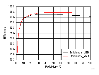
TPS54200 TPS54201 Fig21_efficiency_SLUSCO8.gif
Figure 22. Efficiency
TPS54200 TPS54201 fig23_lusco8.gif
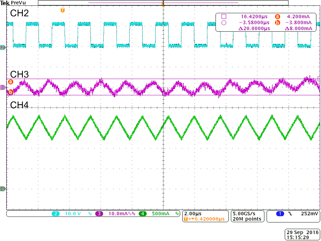
CH2: SW CH3: LED current CH4: Inductor current
(AC-coupled)
Figure 24. LED Current Ripple at 100% PWM Duty Cycle
TPS54200 TPS54201 fig25_lusco8.gif
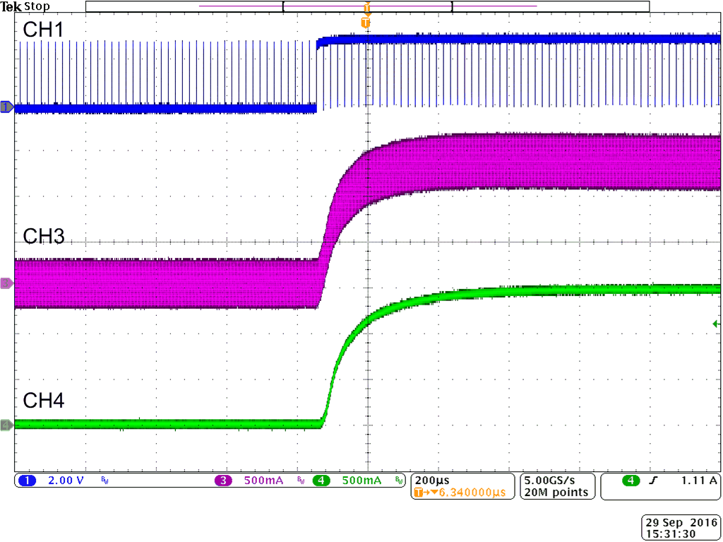
CH1: PWM CH3: Inductor current CH4: LED current
Figure 26. LED Current Transient as PWM Duty Cycle
Changes From 1% to 99%
TPS54200 TPS54201 fig27_lusco8.gif
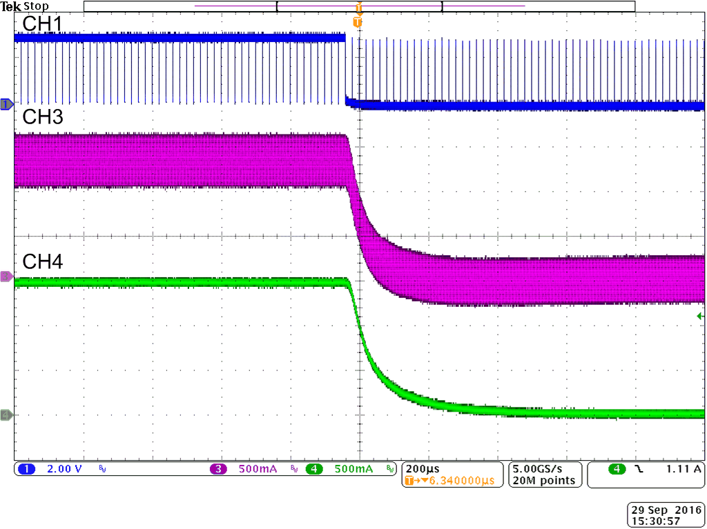
CH1: PWM CH3: Inductor current CH4: LED current
Figure 28. LED Current Transient as PWM Duty Cycle
Changes From 99% to 1%
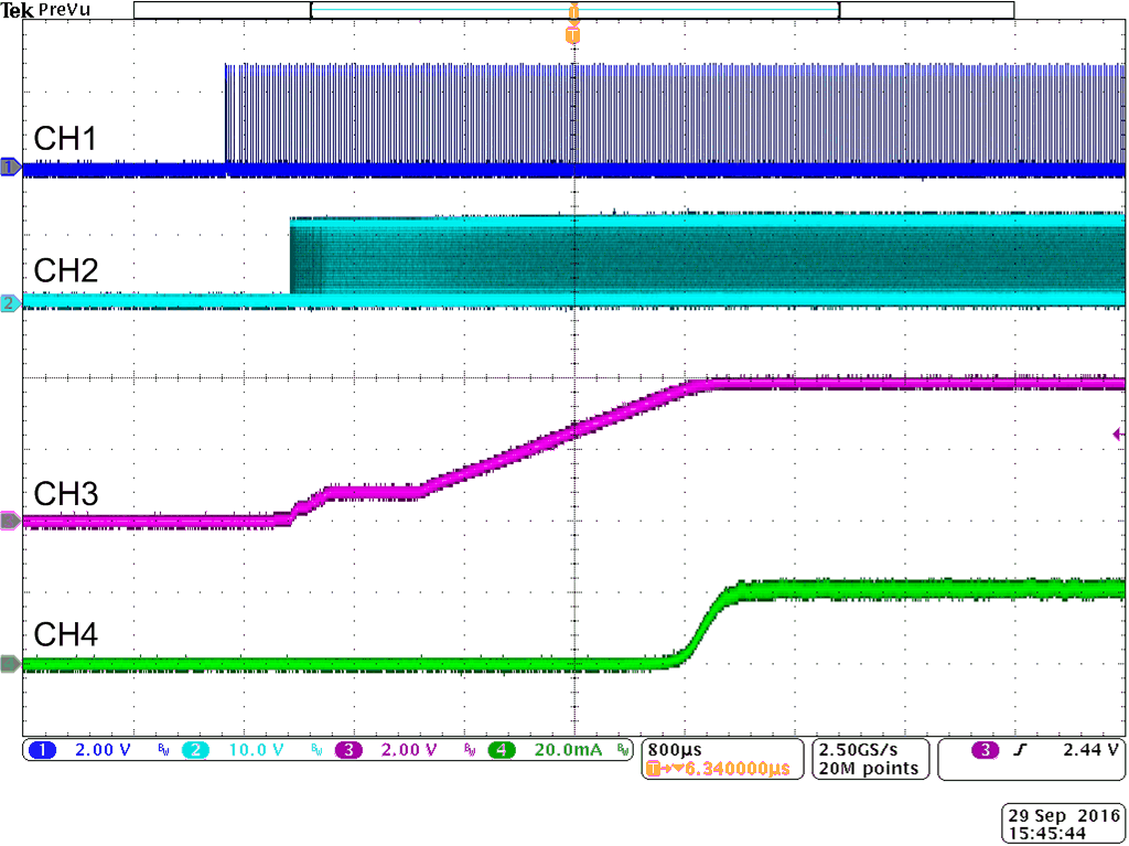
TPS54200 TPS54201 fig29_lusco8.gif
CH1: PWM CH2: SW CH3: VOUT CH4: LED current;
Figure 30. Start-Up at 1% PWM Duty Cycle and 50 kHz
TPS54200 TPS54201 fig31_lusco8.gif
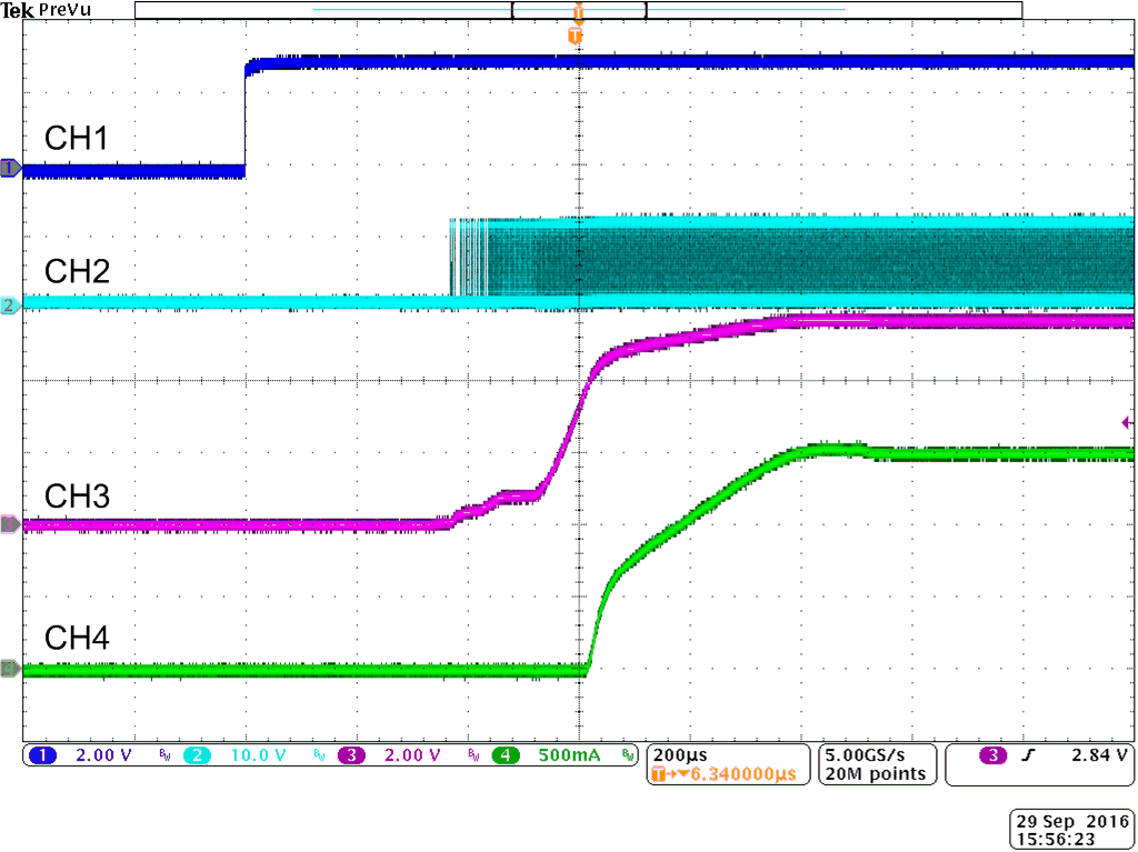
CH1: PWM CH2: SW CH3: VOUT CH4: LED current
Figure 32. Start-Up at 100% PWM Duty Cycle
TPS54200 TPS54201 fig33_lusco8.gif
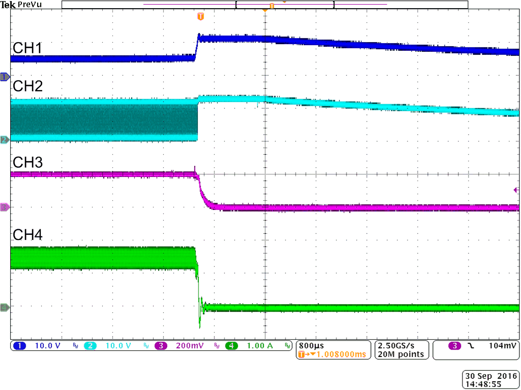
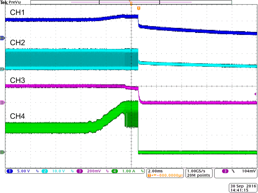
CH1: VOUT CH2: SW CH3: FB CH4: Inductor current
Figure 34. LED Short Protection (100% PWM Duty Cycle) of TPS54200
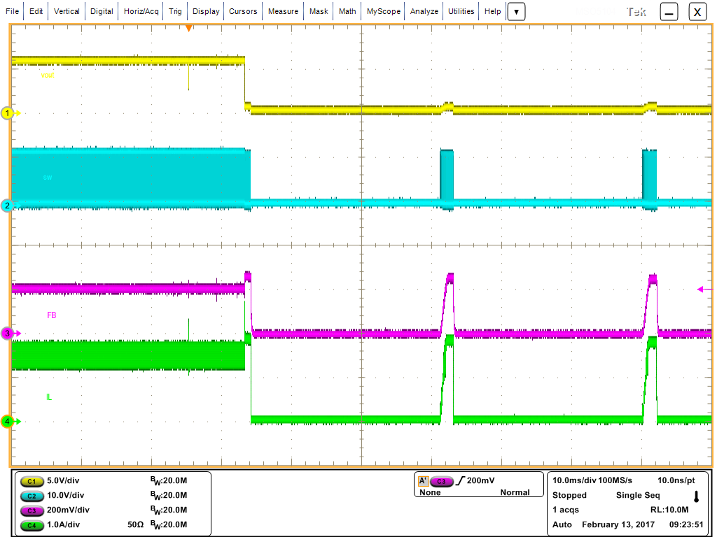
TPS54200 TPS54201 fig34_lusco8.gif
CH1: VOUT CH2: SW CH3: FB CH4: Inductor current
Figure 36. LED Open Protection (100% PWM Duty Cycle) of TPS54200
TPS54200 TPS54201 fig35_lusco8.gif
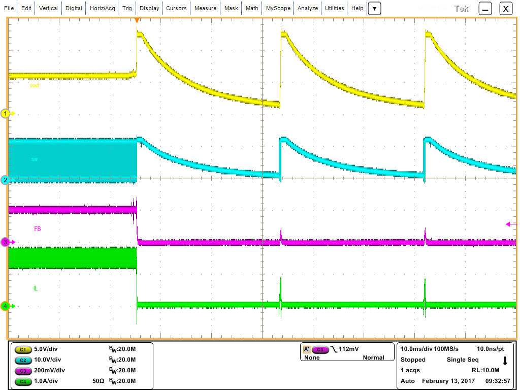
CH1: VOUT CH2: SW CH3: FB CH4:Inductor current
Figure 38. Sense Resistor Short Protection (100% PWM Duty Cycle) of TPS54200
TPS54200 TPS54201 fig22_lusco8.gif
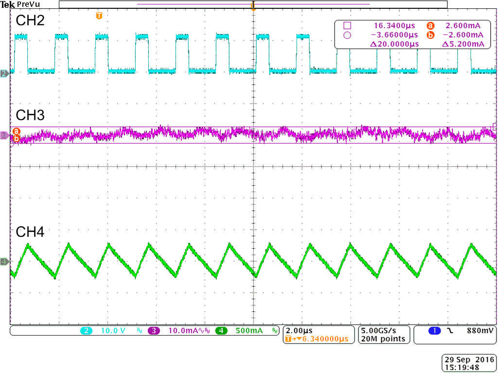
CH2: SW CH3: LED current CH4: Inductor current
(AC-coupled)
Figure 23. LED Current Ripple at 1% PWM Duty Cycle
TPS54200 TPS54201 fig24_lusco8.gif
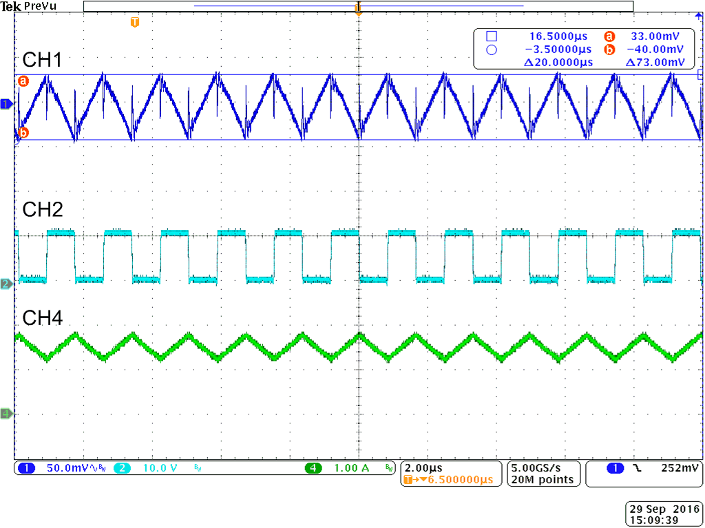
CH1: VVIN CH2: SW CH4: Inductor current
(AC-coupled)
Figure 25. Input Voltage Ripple at 100% PWM Duty Cycle
TPS54200 TPS54201 fig26_lusco8.gif
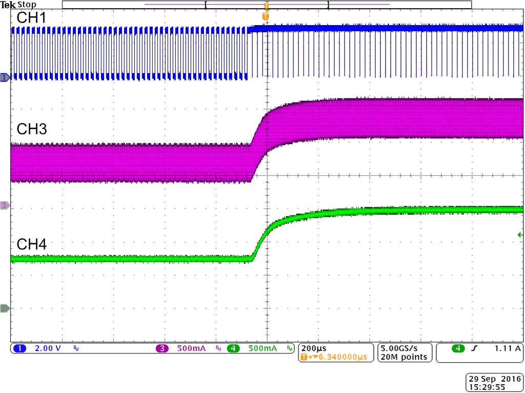
CH1: PWM CH3: Inductor current CH4: LED current
Figure 27. LED Current Transient as PWM Duty Cycle
Changes From 50% to 99%
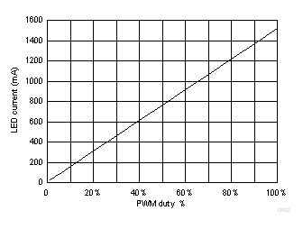
TPS54200 TPS54201 Fig28_LED_Current_vs_PWM_SLUSCO8.gif
Figure 29. LED Current vs PWM Duty Cycle
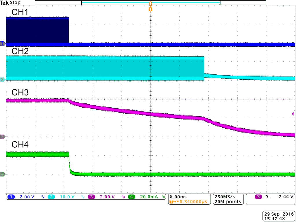
TPS54200 TPS54201 fig30_lusco8.gif
CH1: PWM CH2: SW CH3: VOUT CH4: LED current;
Figure 31. Shutdown at 1% PWM Duty Cycle and 50 kHz
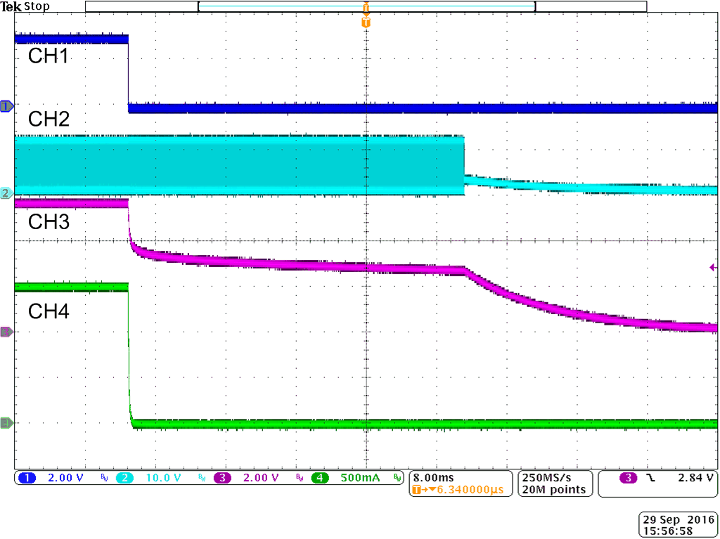
TPS54200 TPS54201 fig32_lusco8.gif
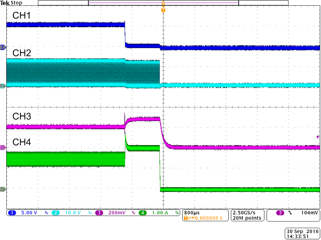
CH1: PWM CH2: SW CH3: VOUT CH4: LED current
Figure 33. Shutdown at 100% PWM Duty Cycle
TPS54200 TPS54201 LED short protection 54201.png
CH1: VOUT CH2: SW CH3: FB CH4: Inductor current
Figure 35. LED Short Protection (100% PWM Duty Cycle) of TPS54201
TPS54200 TPS54201 LED open protection 54201.png
CH1: VOUT CH2: SW CH3: FB CH4: Inductor current
Figure 37. LED Open Protection (100% PWM Duty Cycle) of TPS54201
TPS54200 TPS54201 Rsense Short protection 54201.png
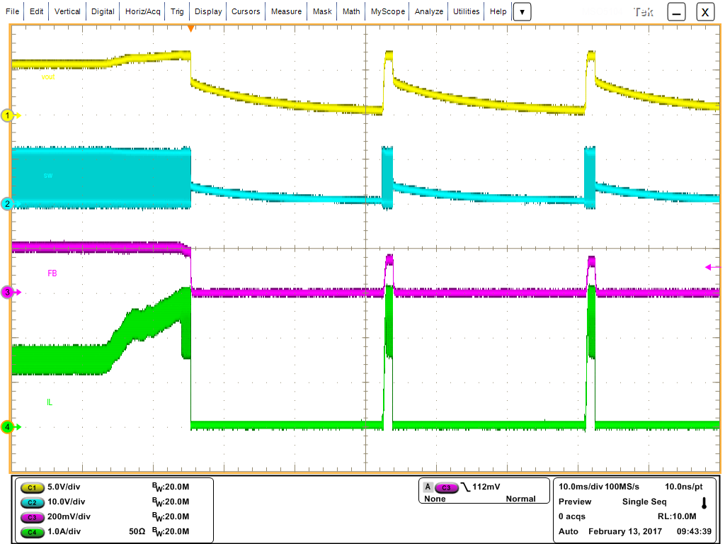
CH1: VOUT CH2: SW CH3: FB CH4: Inductor current
Figure 39. Sense-Resistor Short Protection (100% PWM Duty Cycle) of TPS54201