JAJSBY0G August 2012 – June 2018 TPS54360
PRODUCTION DATA.
- 1 特長
- 2 アプリケーション
- 3 概要
- 4 改訂履歴
- 5 Pin Configuration and Functions
- 6 Specifications
-
7 Detailed Description
- 7.1 Overview
- 7.2 Functional Block Diagram
- 7.3
Feature Description
- 7.3.1 Fixed Frequency PWM Control
- 7.3.2 Slope Compensation Output Current
- 7.3.3 Pulse Skip Eco-mode
- 7.3.4 Low Dropout Operation and Bootstrap Voltage (BOOT)
- 7.3.5 Error Amplifier
- 7.3.6 Adjusting the Output Voltage
- 7.3.7 Enable and Adjusting Undervoltage Lockout
- 7.3.8 Internal Soft-Start
- 7.3.9 Constant Switching Frequency and Timing Resistor (RT/CLK) Terminal)
- 7.3.10 Accurate Current Limit Operation and Maximum Switching Frequency
- 7.3.11 Synchronization to RT/CLK Terminal
- 7.3.12 Overvoltage Protection
- 7.3.13 Thermal Shutdown
- 7.3.14 Small Signal Model for Loop Response
- 7.3.15 Simple Small Signal Model for Peak Current Mode Control
- 7.3.16 Small Signal Model for Frequency Compensation
- 7.4 Device Functional Modes
-
8 Application and Implementation
- 8.1 Application Information
- 8.2
Typical Application
- 8.2.1 Design Requirements
- 8.2.2
Detailed Design Procedure
- 8.2.2.1 Custom Design with WEBENCH® Tools
- 8.2.2.2 Selecting the Switching Frequency
- 8.2.2.3 Output Inductor Selection (LO)
- 8.2.2.4 Output Capacitor
- 8.2.2.5 Catch Diode
- 8.2.2.6 Input Capacitor
- 8.2.2.7 Bootstrap Capacitor Selection
- 8.2.2.8 Undervoltage Lockout Set Point
- 8.2.2.9 Output Voltage and Feedback Resistors Selection
- 8.2.2.10 Minimum VIN
- 8.2.2.11 Compensation
- 8.2.2.12 Discontinuous Conduction Mode and Eco-mode Boundary
- 8.2.2.13 Power Dissipation Estimate
- 8.2.3 Application Curves
- 9 Power Supply Recommendations
- 10Layout
- 11デバイスおよびドキュメントのサポート
- 12メカニカル、パッケージ、および注文情報
パッケージ・オプション
メカニカル・データ(パッケージ|ピン)
- DDA|8
サーマルパッド・メカニカル・データ
- DDA|8
発注情報
7.3.7 Enable and Adjusting Undervoltage Lockout
The TPS54360 is enabled when the VIN terminal voltage rises above 4.3 V and the EN terminal voltage exceeds the enable threshold of 1.2 V. The TPS54360 is disabled when the VIN terminal voltage falls below 4 V or when the EN terminal voltage is below 1.2 V. The EN terminal has an internal pull-up current source, I1, of 1.2 μA that enables operation of the TPS54360 when the EN terminal floats.
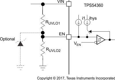
If an application requires a higher undervoltage lockout (UVLO) threshold, use the circuit shown in Figure 22 to adjust the input voltage UVLO with two external resistors. When the EN terminal voltage exceeds 1.2 V, an additional 3.4 μA of hysteresis current, Ihys, is sourced out of the EN terminal. When the EN terminal is pulled below 1.2 V, the 3.4 μA Ihys current is removed. This addional current facilitates adjustable input voltage UVLO hysteresis. Use Equation 4 to calculate RUVLO1 for the desired UVLO hysteresis voltage. Use Equation 5 to calculate RUVLO2 for the desired VIN start voltage.
In applications designed to start at relatively low input voltages (e.g., from 4.5 V to 9 V) and withstand high input voltages (e.g., from 40 V to 60 V), the EN terminal may experience a voltage greater than the absolute maximum voltage of 8.4 V during the high input voltage condition. It is recommended to use a zener diode to clamp the terminal voltage below the absolute maximum rating.
 Figure 22. Adjustable Undervoltage Lockout (UVLO)
