JAJSJU3B May 2020 – June 2021 TPS543820
PRODUCTION DATA
- 1 特長
- 2 アプリケーション
- 3 概要
- 4 Revision History
- 5 Pin Configuration and Functions
- 6 Specifications
-
7 Detailed Description
- 7.1 Overview
- 7.2 Functional Block Diagram
- 7.3
Feature Description
- 7.3.1 VIN Pins and VIN UVLO
- 7.3.2 Enable and Adjustable UVLO
- 7.3.3 Adjusting the Output Voltage
- 7.3.4 Switching Frequency Selection
- 7.3.5 Switching Frequency Synchronization to an External Clock
- 7.3.6 Ramp Amplitude Selection
- 7.3.7 Soft Start and Prebiased Output Start-up
- 7.3.8 Mode Pin
- 7.3.9 Power Good (PGOOD)
- 7.3.10 Current Protection
- 7.3.11 Output Overvoltage and Undervoltage Protection
- 7.3.12 Overtemperature Protection
- 7.3.13 Output Voltage Discharge
- 7.4 Device Functional Modes
-
8 Application and Implementation
- 8.1 Application Information
- 8.2
Typical Applications
- 8.2.1
1.0-V Output, 1-MHz Application
- 8.2.1.1 Design Requirements
- 8.2.1.2
Detailed Design Procedure
- 8.2.1.2.1 Switching Frequency
- 8.2.1.2.2 Output Inductor Selection
- 8.2.1.2.3 Output Capacitor
- 8.2.1.2.4 Input Capacitor
- 8.2.1.2.5 Adjustable Undervoltage Lockout
- 8.2.1.2.6 Output Voltage Resistors Selection
- 8.2.1.2.7 Bootstrap Capacitor Selection
- 8.2.1.2.8 BP5 Capacitor Selection
- 8.2.1.2.9 PGOOD Pullup Resistor
- 8.2.1.2.10 Current Limit Selection
- 8.2.1.2.11 Soft-Start Time Selection
- 8.2.1.2.12 Ramp Selection and Control Loop Stability
- 8.2.1.2.13 MODE Pin
- 8.2.1.3 Application Curves
- 8.2.2 1.0-V Output, 1.5-MHz Application
- 8.2.3 3.3-V Output, 1.0-MHz Application
- 8.2.1
1.0-V Output, 1-MHz Application
- 9 Power Supply Recommendations
- 10Layout
- 11Device and Documentation Support
- 12Mechanical, Packaging, and Orderable Information
8.2.1.2.2 Output Inductor Selection
To calculate the value of the output inductor, use Equation 6. KIND is a ratio that represents the amount of inductor ripple current relative to the maximum output current. The inductor ripple current is filtered by the output capacitor. Therefore, choosing high inductor ripple currents impacts the selection of the output capacitor since the output capacitor must have a ripple current rating equal to or greater than the inductor ripple current. Choosing small inductor ripple currents can degrade the transient response performance. The inductor ripple, KIND, is normally from 0.1 to 0.4 for the majority of applications giving a peak to peak ripple current range of 0.8 A to 3.2 A. The recommended minimum target Iripple is 0.6 A or larger.
For this design example, KIND = 0.2 is used and the inductor value is calculated to be 0.58 µH. An inductor with an inductance of 0.6 µH is selected. It is important that the RMS (Root Mean Square) current and saturation current ratings of the inductor not be exceeded. The RMS and peak inductor current can be found from Equation 8 and Equation 9. For this design, the RMS inductor current is 8 A, and the peak inductor current is 8.8 A. The chosen inductor is a XEL5030-601. It has a saturation current rating of 22 A, an RMS current rating of 21.4 A, and a typical DC series resistance of 4.44 mΩ.
The peak current through the inductor is the inductor ripple current plus the output current. During power up, faults, or transient load conditions, the inductor current can increase above the calculated peak inductor current level calculated in Equation 9. In transient conditions, the inductor current can increase up to the switch current limit of the device. For this reason, the most conservative approach is to specify the current ratings of the inductor based on the switch current limit rather than the steady-state peak inductor current.
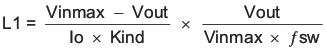
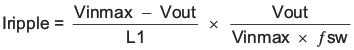
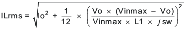
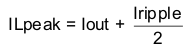
Table 8-2 shows recommended E6 standard inductor values for other common output voltages with a 1-MHz fSW. Using an inductance outside this recommended range typically works but the performance can be affected and should be evaluated. The recommended value is calculated for a nominal input voltage of 12 V. The minimum values are calculated with the maximum input voltage of 18 V. The maximum values are calculated with with an input voltage of 5-V for all but the 5-V output. For the 5-V output, an 8-V input is used.
| OUTPUT VOLTAGE (V) | SWITCHING FREQUENCY (kHz) | MINIMUM INDUCTANCE (µH) | RECOMMENDED INDUCTANCE FOR 8 A (µH) | RECOMMENDED INDUCTANCE FOR 6 A (µH) | MAXIMUM INDUCTANCE (µH) |
|---|---|---|---|---|---|
| 1 | 1000 | 0.33 | 0.47 | 0.47 | 1 |
| 1.8 | 0.47 | 0.68 | 1 | 1.5 | |
| 3.3 | 0.68 | 1 | 1.5 | 1.5 | |
| 5 | 1 | 1.5 | 1.5 | 2.2 |