JAJSJU3B May 2020 – June 2021 TPS543820
PRODUCTION DATA
- 1 特長
- 2 アプリケーション
- 3 概要
- 4 Revision History
- 5 Pin Configuration and Functions
- 6 Specifications
-
7 Detailed Description
- 7.1 Overview
- 7.2 Functional Block Diagram
- 7.3
Feature Description
- 7.3.1 VIN Pins and VIN UVLO
- 7.3.2 Enable and Adjustable UVLO
- 7.3.3 Adjusting the Output Voltage
- 7.3.4 Switching Frequency Selection
- 7.3.5 Switching Frequency Synchronization to an External Clock
- 7.3.6 Ramp Amplitude Selection
- 7.3.7 Soft Start and Prebiased Output Start-up
- 7.3.8 Mode Pin
- 7.3.9 Power Good (PGOOD)
- 7.3.10 Current Protection
- 7.3.11 Output Overvoltage and Undervoltage Protection
- 7.3.12 Overtemperature Protection
- 7.3.13 Output Voltage Discharge
- 7.4 Device Functional Modes
-
8 Application and Implementation
- 8.1 Application Information
- 8.2
Typical Applications
- 8.2.1
1.0-V Output, 1-MHz Application
- 8.2.1.1 Design Requirements
- 8.2.1.2
Detailed Design Procedure
- 8.2.1.2.1 Switching Frequency
- 8.2.1.2.2 Output Inductor Selection
- 8.2.1.2.3 Output Capacitor
- 8.2.1.2.4 Input Capacitor
- 8.2.1.2.5 Adjustable Undervoltage Lockout
- 8.2.1.2.6 Output Voltage Resistors Selection
- 8.2.1.2.7 Bootstrap Capacitor Selection
- 8.2.1.2.8 BP5 Capacitor Selection
- 8.2.1.2.9 PGOOD Pullup Resistor
- 8.2.1.2.10 Current Limit Selection
- 8.2.1.2.11 Soft-Start Time Selection
- 8.2.1.2.12 Ramp Selection and Control Loop Stability
- 8.2.1.2.13 MODE Pin
- 8.2.1.3 Application Curves
- 8.2.2 1.0-V Output, 1.5-MHz Application
- 8.2.3 3.3-V Output, 1.0-MHz Application
- 8.2.1
1.0-V Output, 1-MHz Application
- 9 Power Supply Recommendations
- 10Layout
- 11Device and Documentation Support
- 12Mechanical, Packaging, and Orderable Information
8.2.1.2.1 Switching Frequency
The first step is to decide on a switching frequency. The TPS543820 can operate at five different frequencies from 500 kHz to 2.2 MHz. The fSW is set by the resistor value from the FSEL pin to ground. Typically the highest switching frequency possible is desired because it produces the smallest solution size. A high switching frequency allows for smaller inductors and output capacitors compared to a power supply that switches at a lower frequency. The main tradeoff made with selecting a higher switching frequency is extra switching power loss, which hurts the efficiency of the regulator.
The maximum switching frequency for a given application can be limited by the minimum on-time of the regulator. The maximum fSW can be estimated with Equation 4. Using the maximum minimum on-time of 40 ns and 13.2-V maximum input voltage for this application, the maximum switching frequency is 1890 kHz. The selected switching frequency must also consider the tolerance of the switching frequency. A switching frequency of 1000 kHz was selected for a good balance of solution size and efficiency. To set the frequency to 1000 kHz, the selected FSEL resistor is 11.8 kΩ per Table 7-1.
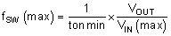
Figure 8-2 shows the maximum recommended input voltage versus output voltage for each FSEL frequency. This graph uses a minimum on-time of 45 ns and includes the 10% tolerance of the switching frequency. A minimum on-time of 45 ns is used in this graph to provide margin to the minimum controllable on-time to ensure pulses are not skipped at no load. At light loads, the dead-time between the low-side MOSFET turning off and high-side MOSFET turning on contributes to the minimum SW node pulse-width.
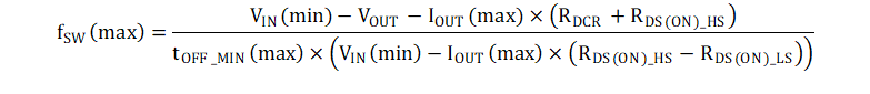
In high output voltage applications, the minimum off-time must also be considered when selecting the switching frequency. When hitting the minimum off-time limits, the operating duty cycle will max out and the output voltage will begin to drop with the input voltage. Equation 5 calculates the maximum switching frequency to avoid this limit. This equation requires the DC resistance of the inductor, RDCR, selected in the following step. A preliminary estimate of 10 mΩ can be used but this should be recalculated based on the specifications of the inductor selected. If operating near the maximum fSW limited by the minimum off-time, the increase in resistance at higher temperature must be considered.