JAJS364F May 2009 – May 2017 TPS54620
PRODUCTION DATA.
- 1 特長
- 2 アプリケーション
- 3 概要
- 4 改訂履歴
- 5 Pin Configurations and Functions
- 6 Specifications
-
7 Detailed Description
- 7.1 Overview
- 7.2 Functional Block Diagram
- 7.3
Feature Description
- 7.3.1 Fixed Frequency PWM Control
- 7.3.2 Continuous Current Mode Operation (CCM)
- 7.3.3 VIN and Power VIN Pins (VIN and PVIN)
- 7.3.4 Voltage Reference
- 7.3.5 Adjusting the Output Voltage
- 7.3.6 Safe Start-Up into Prebiased Outputs
- 7.3.7 Error Amplifier
- 7.3.8 Slope Compensation
- 7.3.9 Enable and Adjusting Undervoltage Lockout
- 7.3.10 Adjustable Switching Frequency and Synchronization (RT/CLK)
- 7.3.11 Slow Start (SS/TR)
- 7.3.12 Power Good (PWRGD)
- 7.3.13 Output Overvoltage Protection (OVP)
- 7.3.14 Overcurrent Protection
- 7.3.15 Thermal Shutdown
- 7.3.16 Small Signal Model for Loop Response
- 7.3.17 Simple Small Signal Model for Peak Current Mode Control
- 7.3.18 Small Signal Model for Frequency Compensation
- 7.4 Device Functional Modes
-
8 Application and Implementation
- 8.1 Application Information
- 8.2
Typical Application
- 8.2.1 Design Requirements
- 8.2.2
Detailed Design Procedures
- 8.2.2.1 Custom Design With WEBENCH Tools
- 8.2.2.2 Operating Frequency
- 8.2.2.3 Output Inductor Selection
- 8.2.2.4 Output Capacitor Selection
- 8.2.2.5 Input Capacitor Selection
- 8.2.2.6 Slow-Start Capacitor Selection
- 8.2.2.7 Bootstrap Capacitor Selection
- 8.2.2.8 Undervoltage Lockout Set Point
- 8.2.2.9 Output Voltage Feedback Resistor Selection
- 8.2.2.10 Compensation Component Selection
- 8.2.2.11 Fast Transient Considerations
- 8.2.3 Application Curves
- 9 Power Supply Recommendations
- 10Layout
- 11デバイスおよびドキュメントのサポート
- 12メカニカル、パッケージ、および注文情報
パッケージ・オプション
デバイスごとのパッケージ図は、PDF版データシートをご参照ください。
メカニカル・データ(パッケージ|ピン)
- RHL|14
- RGY|14
サーマルパッド・メカニカル・データ
発注情報
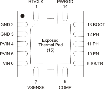
5 Pin Configurations and Functions
Pin Functions
| PIN | I/O(1) | DESCRIPTION | |
|---|---|---|---|
| NAME | NO. | ||
| RT/CLK | 1 | I | Automatically selects between RT mode and CLK mode. An external timing resistor adjusts the switching frequency of the device; in CLK mode, the device synchronizes to an external clock. |
| GND | 2, 3 | G | Return for control circuitry and low-side power MOSFET. |
| PVIN | 4, 5 | P | Power input. Supplies the power switches of the power converter. |
| VIN | 6 | P | Supplies the control circuitry of the power converter. |
| VSENSE | 7 | I | Inverting input of the gm error amplifier. |
| COMP | 8 | O | Error amplifier output, and input to the output switch current comparator. Connect frequency compensation to this pin. |
| SS/TR | 9 | O | Slow-start and tracking. An external capacitor connected to this pin sets the internal voltage reference rise time. The voltage on this pin overrides the internal reference. It can be used for tracking and sequencing. |
| EN | 10 | I | Enable pin. Float to enable. Adjust the input undervoltage lockout with two resistors. |
| PH | 11, 12 | O | Switch node. |
| BOOT | 13 | I | A bootstrap cap is required between BOOT and PH. The voltage on this cap carries the gate drive voltage for the high-side MOSFET. |
| PWRGD | 14 | G | Power Good fault pin. Asserts low if output voltage is low because of thermal shutdown, dropout, over-voltage, EN shutdown, or during slow start. |
| Exposed Thermal PAD | 15 | G | Thermal pad of the package and signal ground and it must be soldered down for proper operation. |
(1) I = input, O = output, G = GND, P = Power
