SGLS276D January 2005 – March 2016 TPS61040-Q1 , TPS61041-Q1
PRODUCTION DATA.
- 1 Features
- 2 Applications
- 3 Description
- 4 Revision History
- 5 Pin Configuration and Functions
- 6 Specifications
- 7 Detailed Description
- 8 Application and Implementation
- 9 Power Supply Recommendations
- 10Layout
- 11Device and Documentation Support
- 12Mechanical, Packaging, and Orderable Information
パッケージ・オプション
デバイスごとのパッケージ図は、PDF版データシートをご参照ください。
メカニカル・データ(パッケージ|ピン)
- DBV|5
サーマルパッド・メカニカル・データ
発注情報
10 Layout
10.1 Layout Guidelines
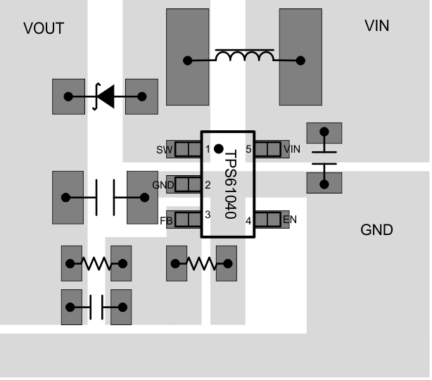
Typical for all switching power supplies, the layout is an important step in the design; especially at high peak currents and switching frequencies. If the layout is not carefully done, the regulator can show noise problems and duty cycle jitter.
Figure 23 provides an example of layout design with TPS6104x-Q1 device.
- The input capacitor must be placed as close as possible to the input pin for good input voltage filtering.
- The inductor and diode must be placed as close as possible to the switch pin to minimize the noise coupling into other circuits.
- Keeping the switching pin and plane area short helps in minimizing the radiated emissions. It is also important to have very low impedance switch plane to reduce the switching losses and hence a trade-off must be made between these two and the switching pin and plane must be optimized.
- Because the feedback pin and network is noise-sensitive, the feedback network must be routed away from the inductor.
- The feedback pin and feedback network must be shielded with a ground plane or trace to minimize noise coupling into this circuit.
- A star ground connection or ground plane minimizes ground shifts and noise.
