SLVS441D December 2002 – December 2014 TPS61042
PRODUCTION DATA.
- 1 Features
- 2 Applications
- 3 Description
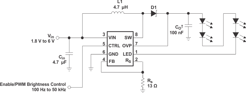
- 4 Typical Application
- 5 Revision History
- 6 Pin Configuration and Functions
- 7 Specifications
- 8 Detailed Description
- 9 Application and Implementation
- 10Power Supply Recommendations
- 11Layout
- 12Device and Documentation Support
- 13Mechanical, Packaging, and Orderable Information
1 Features
- Current Source With Overvoltage Protection
- Input Voltage Range: 1.8 V to 6 V
- Internal 30 V Switch
- Up to 85% Efficiency
- Precise Brightness Control Using PWM Signal or Analog Signal
- Switching Frequency: Up to 1 MHz
- Internal Power MOSFET Switch: 500 mA
- Operates With Small Output Capacitors Down to 100 nF
- Disconnects LEDs During Shutdown
- No Load Quiescent Current: 38 µA Typ
- Shutdown Current: 0.1 µA Typ
- Available in a Small 3 mm × 3 mm QFN Package
2 Applications
- White LED Supply for Backlight/Sidelight Displays
- PDA, Pocket PC, Smart Phones
- Handheld Devices
- Cellular Phones
3 Description
The TPS61042 is a high frequency boost converter with constant current output that drives white LEDs or similar. The LED current is set with the external sense resistor (RS) and is directly regulated by the feedback pin (FB) that regulates the voltage across the sense resistor RS to 252 mV (typ). To control LED brightness, the LED current can be pulsed by applying a PWM (pulse width modulated) signal with a frequency range of 100 Hz to 50 kHz to the control pin (CTRL). To allow higher flexibility, the device can be configured where the brightness can be controlled by an analog signal as well, as described in the application information section. To avoid possible leakage currents through the LEDs during shutdown, the control pin (CTRL) disables the device and disconnects the LEDs from ground. For maximum safety during operation, the output has integrated overvoltage protection that prevents damage to the device in case of a high impedance output (e.g. faulty LED).
Device Information(1)
| PART NUMBER | PACKAGE | BODY SIZE (NOM) |
|---|---|---|
| TPS61042 | SON (8) | 3.00 mm × 3.00 mm |
- For all available packages, see the orderable addendum at the end of the data sheet.
4 Typical Application