SLVS440C January 2003 – December 2014 TPS61045
PRODUCTION DATA.
- 1 Features
- 2 Applications
- 3 Description
- 4 Revision History
- 5 Pin Configuration and Functions
- 6 Specifications
- 7 Detailed Description
- 8 Application and Implementation
- 9 Power Supply Recommendations
- 10Layout
- 11Device and Documentation Support
- 12Mechanical, Packaging, and Orderable Information
パッケージ・オプション
デバイスごとのパッケージ図は、PDF版データシートをご参照ください。
メカニカル・データ(パッケージ|ピン)
- DRB|8
サーマルパッド・メカニカル・データ
- DRB|8
発注情報
8 Application and Implementation
NOTE
Information in the following applications sections is not part of the TI component specification, and TI does not warrant its accuracy or completeness. TI’s customers are responsible for determining suitability of components for their purposes. Customers should validate and test their design implementation to confirm system functionality.
8.1 Application Information
The TPS61045 device is a high-frequency boost converter with digitally-programmable output voltage and true shutdown. The TPS61045 device operates with an input voltage range of 1.8 to 6 V and generates output voltages up to 28 V. The device operates in a constant peak current control, which maintains high efficiency over the entire load current range, and with a typical switching frequency of up to 1 MHz.
8.2 Typical Application
The following section provides a step-by-step design approach for configuring the TPS61045 as a voltage regulating boost converter, as shown in Figure 12.
8.2.1 Analog Adjusted Output Voltage
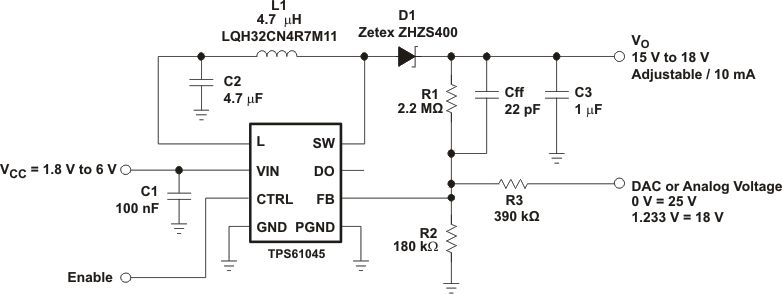 Figure 12. Typical Application With Analog Adjusted Output Voltage
8.2.1.1 Design Requirements
Table 3. Design Parameters
| PARAMETERS | VALUES |
|---|---|
| Output voltage | 18 V |
| Input voltage | 1.8 to 6 V |
| Output current | 10 mA |
8.2.1.2 Detailed Design Procedure
8.2.1.2.1 Inductor Selection, Maximum Load Current
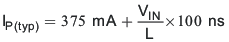
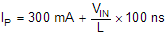
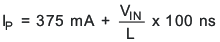
Because the PFM peak current control scheme is inherently stable, the inductor and capacitor value does not affect the stability of the regulator. The selection of the inductor together with the nominal load current, input, and output voltage of the application determines the switching frequency of the converter. Depending on the application, TI recommends inductor values between 2.2 to 47 μH. The maximum inductor value is determined by the maximum switch on-time of 6 μs (typical). The peak current limit of 375 mA (typical) must be reached within 6 μs for proper operation.
The inductor value determines the maximum switching frequency of the converter. Therefore, the user must select the inductor value for the maximum switching frequency at maximum load current of the converter and should not be exceeded. A good inductor value to start with is 4.7 μH. The maximum switching frequency is calculated as:
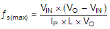
where
- IP = Peak current as described in Peak Current Control
where
- L = Selected inductor value; TI recommends inductor values between 2.2 to 47 μH
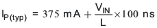
If the selected inductor does not exceed the maximum switching frequency of the converter, as a next step, the switching frequency at the nominal load current is estimated as follows:
where
- IP = Peak current as described in Peak Current Control
where
- L = Selected inductor value
- I(LOAD) = Nominal load current
- VF = Rectifier diode forward voltage (typically 0.3 V)
The smaller the inductor value, the higher the switching frequency of the converter, but the lower the efficiency.
The maximum load current of the converter is determined at the operation point where the converter starts to enter continuous conduction mode. The converter must always operate in DCM to maintain regulation.
Two conditions exist for determining the maximum output current of the converter. One condition is when the inductor current fall time is <400 ns, and the other condition is when the inductor current fall time is >400 ns.
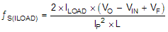
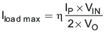
One way to calculate the maximum available load current for certain operation conditions is to estimate the expected converter efficiency at the maximum load current. Find this number in the efficiency graphs shown in Figure 1 and Figure 2. Then, the maximum load current can be estimated:
Inductor fall time:
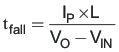
For tf ≥ 400 ns:
For tf ≤ 400 ns:
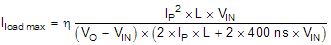
where
- L = Selected inductor value
- η = Expected converter efficiency (typically between 70% to 85%)
- IP = Peak current as described in Peak Current Control
Equation 10 contains the expected converter efficiency that allows calculating the expected maximum load current the converter can support. Find the efficiency in the efficiency graphs shown in Figure 1 and Figure 2, or 80% can be used as a good estimation.
The selected inductor must have a saturation current which meets the maximum peak current of the converter as calculated in Peak Current Control. Use the maximum value for ILim (450 mA) for this calculation.
Another important inductor parameter is the dc resistance. The lower the dc resistance, the higher the efficiency of the converter. See Table 4 and Inductor Selection, Maximum Load Current.
Table 4. Possible Inductor Selection
| Inductor Value | Component Supplier | Comments |
|---|---|---|
| 10 μH | Sumida CR32-100 | High efficiency |
| 10 μH | Sumida CDRH3D16-100 | High efficiency |
| 10 μH | Murata LQH43CN100K01 | |
| 4.7 μH | Sumida CDRH3D16-4R7 | Small solution size |
| 4.7 μH | Murata LQH32CN4R7M51 | Small solution size |
8.2.1.2.2 Setting the Output Voltage
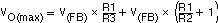
See Simplified Schematic. When the converter is programmed to the minimum output voltage, the DAC output (DO) equals the reference voltage of 1.233 V (typical). Therefore, only the feedback resistor network (R1) and (R2) determines the output voltage under these conditions. This gives the minimum output voltage possible and can be calculated as:
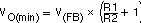
The maximum output voltage is determined as the DAC output (DO) is set to 0 V:
The output voltage can be digitally programmed by pulling the CTRL pin low for a certain period of time as described in Digital Interface (CTRL). Pulling the signal applied to the CTRL pin low and high again (for related timing see Electrical Characteristics) increases or decreases the DAC output DO (pin 3) one step where one step is typically 19.6 mV. A voltage step on DO of 19.6 mV (typical) changes the output voltage by one step and is calculated as:

The possible output voltage range is determined by selecting R1, R2, and R3. A possible larger output voltage range gives a larger output voltage step size. The smaller the possible output voltage range, the smaller the output voltage step size.
To reduce the overall operating quiescent current in battery-powered applications a high-impedance voltage divider must be used with a typical value for R2 of ≤200 kΩ and a maximum value for R1 of 2.2 MΩ.
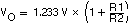
Some applications may not need the digital interface to program the output voltage. In this case, the output DO can be left open as shown in Figure 12, and the output voltage is calculated as for any standard boost converter:
In such a configuration, a high-impedance voltage divider must also be used to minimize ground current, and TI recommends a typical value for R2 of ≤200 kΩ and a maximum value for R1 of 2.2 MΩ.
A feed-forward capacitor (C(FF)), across the upper feedback resistor (R1), is required to provide sufficient overdrive for the error comparator. Without a feed-forward capacitor or with a too-small feed-forward capacitor value, the device shows double pulses or a pulse burst instead of single pulses at the switch node (SW). This can cause higher output voltage ripple. If a higher output voltage ripple is acceptable, the feed-forward capacitor can be left out also.
The lower the switching frequency of the converter, the larger the feed-forward capacitor value needs to be. A good starting point is to use a 10-pF feed-forward capacitor. As a first estimation, the required value for the feed-forward capacitor can be calculated at the operation point:
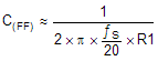
where
- R1 = Upper resistor of voltage divider
- ƒS = Switching frequency of the converter at the nominal load current. (For the calculation of the switching frequency, see Inductor Selection, Maximum Load Current.)
For C(FF), choose a value which comes closest to the calculation result.
The larger the feed-forward capacitor, the worse the line regulation of the device. Therefore, select the feed-forward capacitor as small as possible if good line regulation is of concern.
8.2.1.2.3 Output Capacitor Selection
For better output voltage filtering, TI recommends a low-ESR output capacitor. Ceramic capacitors have low-ESR values, but depending on the application, tantalum capacitors can also be used. For the selection of the output capacitor, see Table 5.
Assuming the converter does not show double pulses or pulse bursts on the switch node (SW), the output voltage ripple is calculated as:
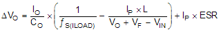
where
- IP = Peak current as described in Peak Current Control
where
- L = Selected inductor value
- IO(LOAD)= Nominal load current
- ƒS(ILoad) = Switching frequency at the nominal load current as calculated previously.
- VF = Rectifier diode forward voltage (typically 0.3 V)
- CO = Selected output capacitor
- ESR = Output capacitor ESR value
8.2.1.2.4 Input Capacitor Selection
The input capacitor (C1) filters the high-frequency noise to the control circuit and must be directly connected to the input pin (VIN) of the device. The capacitor (C2) connected to the L pin of the device is the input capacitor for the power stage.
The main purpose of the capacitor (C2), that is connected directly to the L pin, is to smooth the inductor current. A larger capacitor reduces the inductor ripple current present at the L pin. The smaller the ripple current at the L pin, the higher the efficiency of the converter. If a sufficiently large capacitor is used, the input switch must carry only the dc current, filtered by the capacitor (C2), and not the high switching currents of the converter. A 4.7- or 10-μF ceramic capacitor (C2) is sufficient for most applications. For better filtering, this value can be increased without limit. See Table 5 for input capacitor recommendations.
Table 5. Possible Input and Output Capacitor Selection
| Capacitor | Voltage Rating | Component Supplier | Comments |
|---|---|---|---|
| 4.7 F/X5R/0805 | 6.3 V | Tayo Yuden JMK212BY475MG | CI / CO |
| 10 μF/X5R/0805 | 6.3 V | Tayo Yuden JMK212BJ106MG | CI / CO |
| 1 μF/X7R/1206 | 25 V | Tayo Yuden TMK316BJ105KL | CO |
| 1 μF/X7R/1206 | 35 V | Tayo Yuden GMK316BJ105KL | CO |
| 4.7 μF/X5R/1210 | 25 V | Tayo Yuden TMK325BJ475MG | CO |
8.2.1.2.5 Diode Selection
To achieve high efficiency, use a Schottky diode. The current rating of the diode must meet the peak current rating of the converter as it is calculated in Peak Current Control. Use the maximum value for I(LIM) (450 mA) for this calculation. For the selection of the Schottky diode, see Table 6.
Table 6. Possible Schottky Diode Selection
| Component Supplier | Reverse Voltage |
|---|---|
| ON Semiconductor MBR0530 | 30 V |
| ON Semiconductor MBR0520 | 20 V |
| ON Semiconductor MBRM120L | 20 V |
| Toshiba CRS02 | 30 V |
| Zetex ZHZS400 | 40 V |
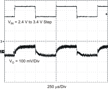
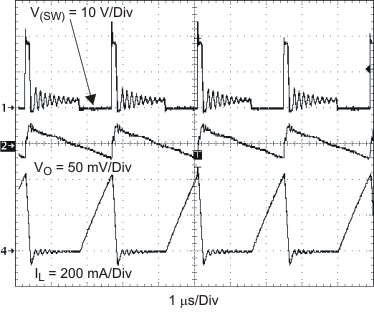
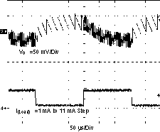
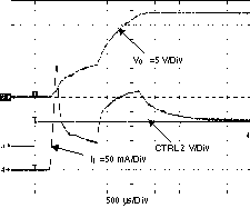
8.2.1.3 Application Curves
8.2.2 OLED Supply with Higher Output Current
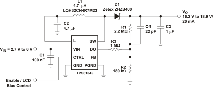 Figure 17. OLED Supply Providing Higher Output Current
8.2.2.1 Design Requirements
Table 7. Design Parameters
| PARAMETERS | VALUES |
|---|---|
| Output voltage | 16.2 to 18.9 V |
| Input voltage | 2.7 to 6 V |
| Output current | 20 mA |
8.2.2.2 Detailed Design Procedure
Refer to the prior Detailed Design Procedure.
8.2.2.3 Application Curves
Refer to waveforms in the prior Application Curves.