SLVS440C January 2003 – December 2014 TPS61045
PRODUCTION DATA.
- 1 Features
- 2 Applications
- 3 Description
- 4 Revision History
- 5 Pin Configuration and Functions
- 6 Specifications
- 7 Detailed Description
- 8 Application and Implementation
- 9 Power Supply Recommendations
- 10Layout
- 11Device and Documentation Support
- 12Mechanical, Packaging, and Orderable Information
パッケージ・オプション
デバイスごとのパッケージ図は、PDF版データシートをご参照ください。
メカニカル・データ(パッケージ|ピン)
- DRB|8
サーマルパッド・メカニカル・データ
- DRB|8
発注情報
10 Layout
10.1 Layout Guidelines
As for all switching power supplies, the layout is an important step in the design, especially at high peak currents and switching frequencies. If the layout is not carefully implemented, the regulator can show noise problems and duty cycle jitter.
The inductor and diode must be placed as close as possible to the switch pin (SW) to minimize noise coupling into other circuits. Because the feedback pin and network is a high-impedance circuit, the feedback network must be routed away from the inductor. Also, the input capacitor must be placed as close as possible to the input pin for good input-voltage filtering. If space is critical and these guidelines can not be followed completely, the user must give the highest priority to the close placement of the diode to the switch pin (SW).
10.2 Layout Example
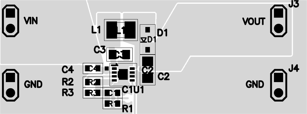 Figure 18. Board Layout Example
10.3 Thermal Considerations
The TPS61045 device is available in a thermally-enhanced VSON package. The package includes a thermal pad, improving the thermal capabilities of the package. See VSON PCB attachment application note (SLUA271).
The thermal resistance junction to ambient (RΘJA) of the VSON package depends on the PCB layout. Use thermal vias and wide PCB traces to improve thermal resistance (RΘJA). Under normal operation conditions, no PCB vias are required for the thermal pad. However, the thermal pad must be soldered to the PCB.